JAJSGR0F December 2010 – December 2018 TPS51916
PRODUCTION DATA.
- 1 特長
- 2 アプリケーション
- 3 概要
- 4 改訂履歴
- 5 概要(続き)
- 6 Pin Configuration and Functions
- 7 Specifications
-
8 Detailed Description
- 8.1 Overview
- 8.2 Functional Block Diagram
- 8.3
Feature Description
- 8.3.1 VDDQ Switch Mode Power Supply Control
- 8.3.2 VREF and REFIN, VDDQ Output Voltage
- 8.3.3 Soft-Start and Powergood
- 8.3.4 Power State Control
- 8.3.5 Discharge Control
- 8.3.6 VTT and VTTREF
- 8.3.7 VDDQ Overvoltage and Undervoltage Protection
- 8.3.8 VDDQ Out-of-Bound Operation
- 8.3.9 VDDQ Overcurrent Protection
- 8.3.10 VTT Overcurrent Protection
- 8.3.11 V5IN Undervoltage Lockout Protection
- 8.3.12 Thermal Shutdown
- 8.4 Device Functional Modes
- 8.5 D-CAP2™ Mode Operation
- 9 Application and Implementation
- 10Power Supply Recommendations
- 11Layout
- 12デバイスおよびドキュメントのサポート
- 13メカニカル、パッケージ、および注文情報
7.6 Typical Characteristics
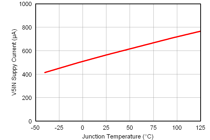 Figure 1. V5IN Supply Current vs Junction Temperature
  Figure 3. VLDOIN Supply Current vs Junction Temperature
  Figure 5. OVP/UVP Threshold vs Junction Temperature
 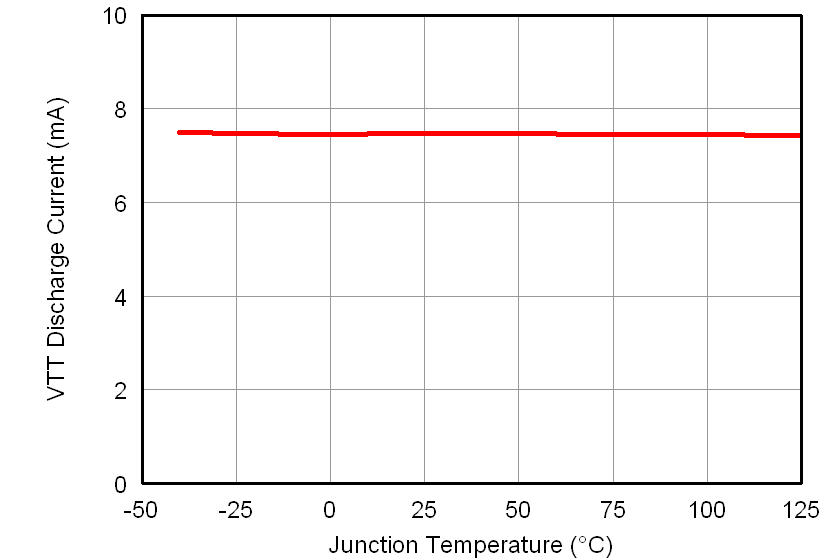 Figure 7. VTT Discharge Current vs Junction Temperature
  Figure 9. Switching Frequency vs Input Voltage
  Figure 11. Switching Frequency vs Input Voltage
  Figure 13. Switching Frequency vs Load Current
 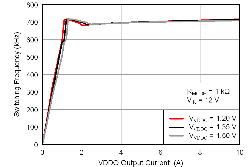 Figure 15. Switching Frequency vs Load Current
 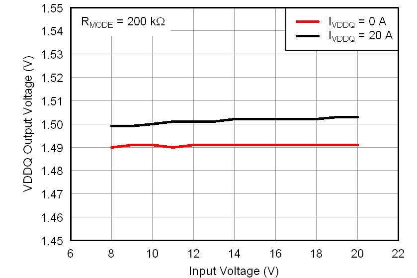 Figure 17. Line Regulation
  Figure 19. VTTREF Load Regulation
 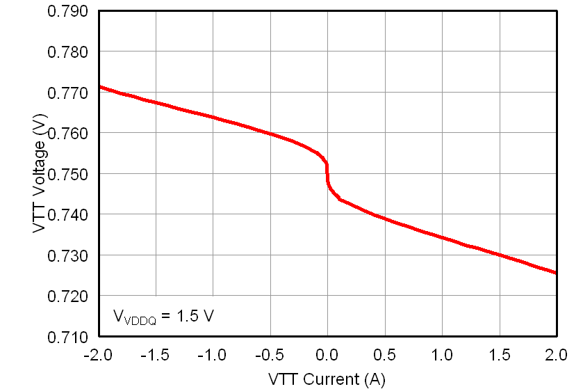 Figure 21. VTT Load Regulation
 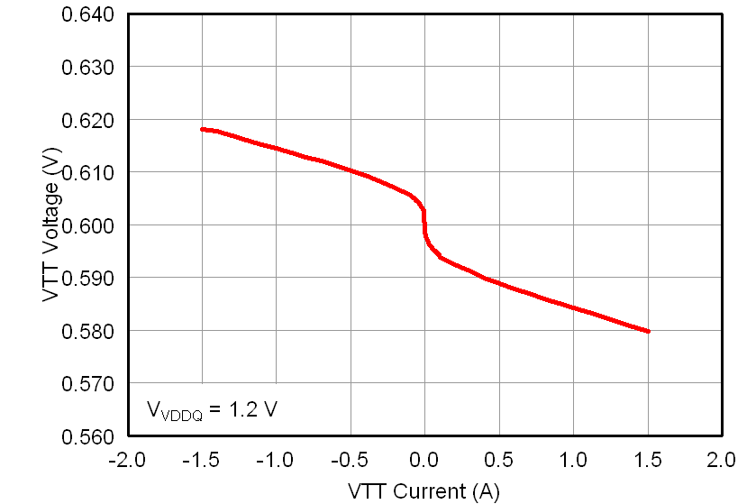 Figure 23. VTT Load Regulation
  Figure 25. 1.5-V Load Transient Response
  Figure 27. 1.5-V Startup Waveforms
 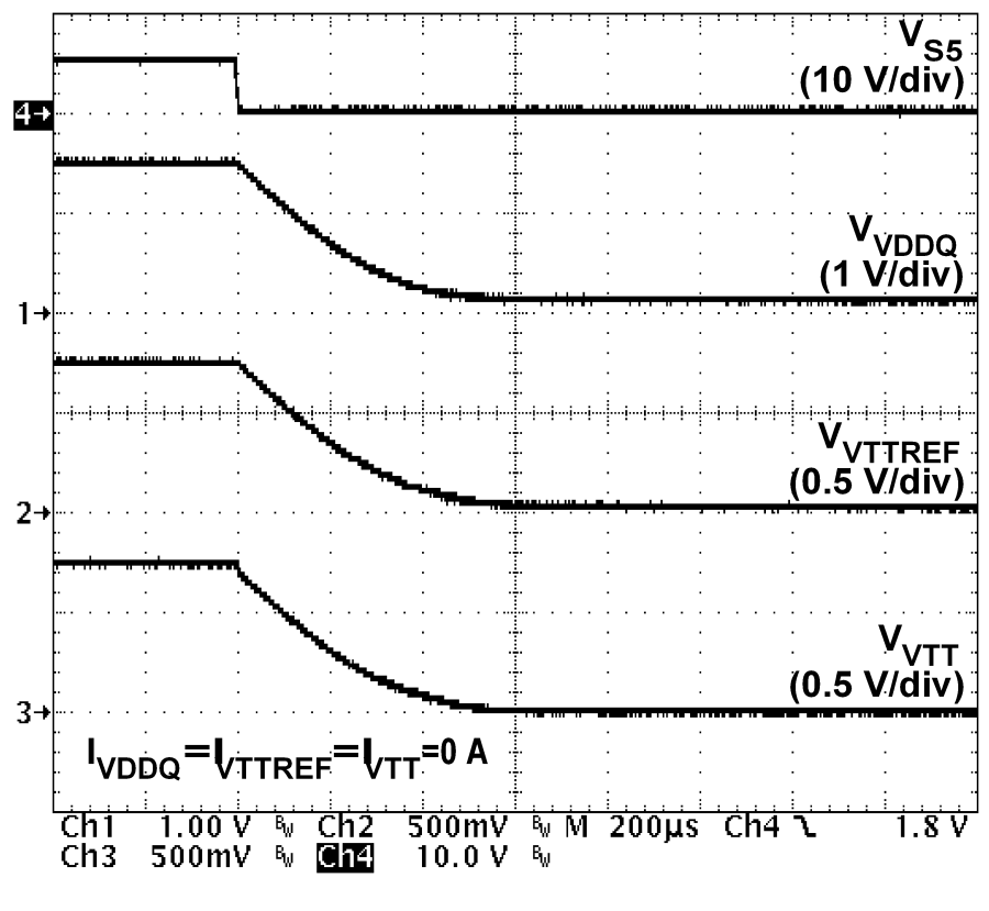 Figure 29. 1.5-V Soft-Stop Waveforms (Tracking Discharge)
  Figure 31. VDDQ Bode Plot
  Figure 33. VTT Bode Plot (Source)
  Figure 2. V5IN Shutdown Current vs Junction Temperature
 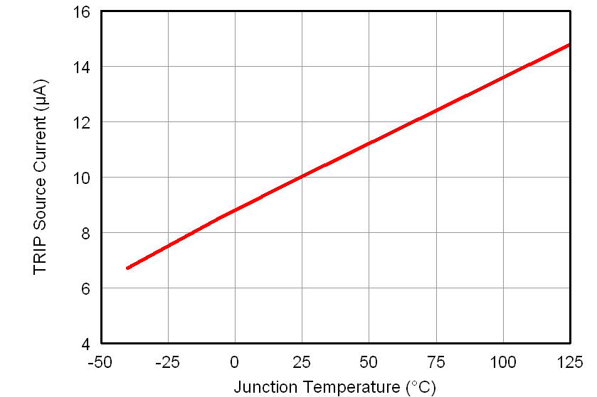 Figure 4. Current Sense Current vs Junction Temperature
 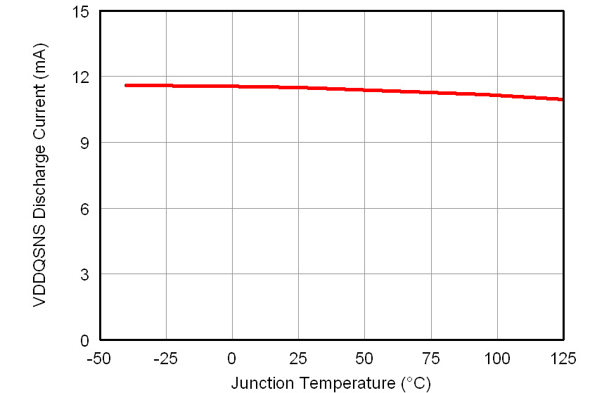 Figure 6. VDDQSNS Discharge Current vs Junction Temperature
  Figure 8. Switching Frequency vs Input Voltage
 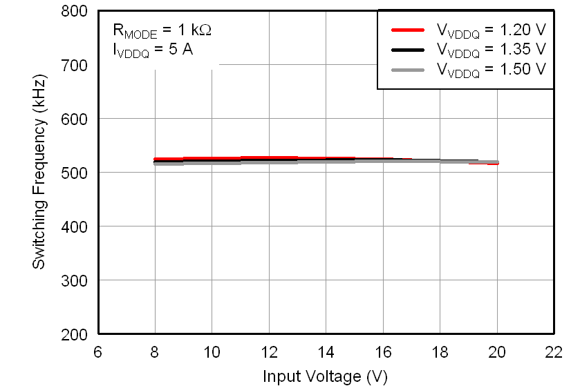 Figure 10. Switching Frequency vs Input Voltage
 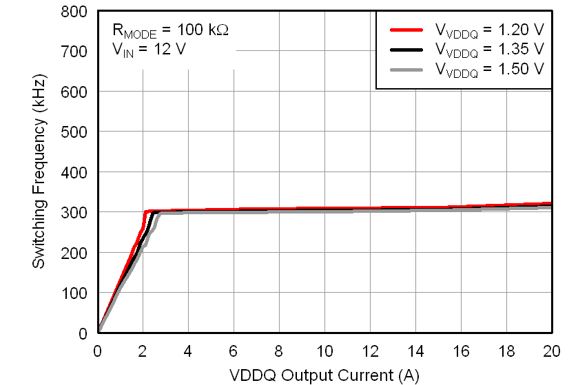 Figure 12. Switching Frequency vs Load Current
 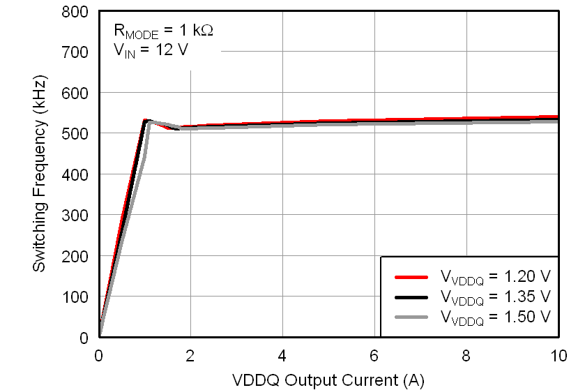 Figure 14. Switching Frequency vs Load Current
  Figure 16. Load Regulation
  Figure 18. VTTREF Load Regulation
 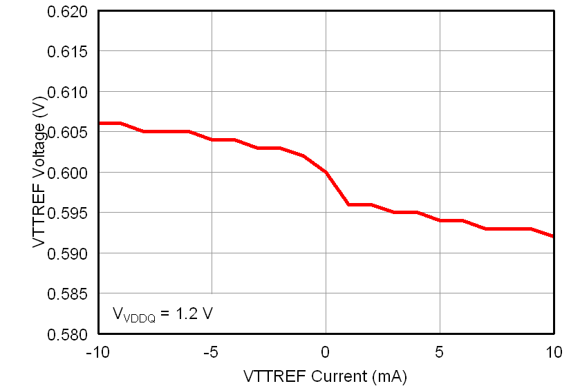 Figure 20. VTTREF Load Regulation
 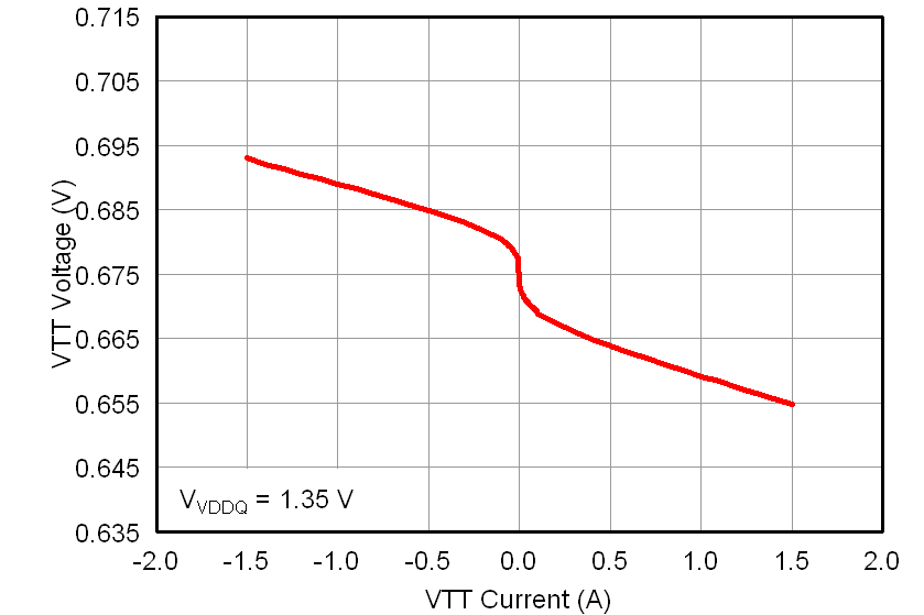 Figure 22. VTT Load Regulation
 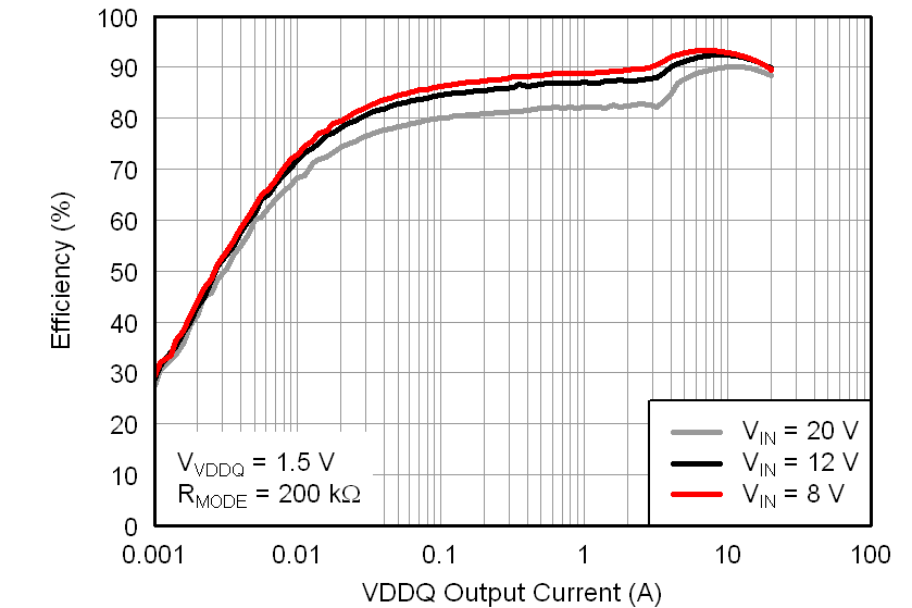 Figure 24. Efficiency
  Figure 26. VTT Load Transient Response
 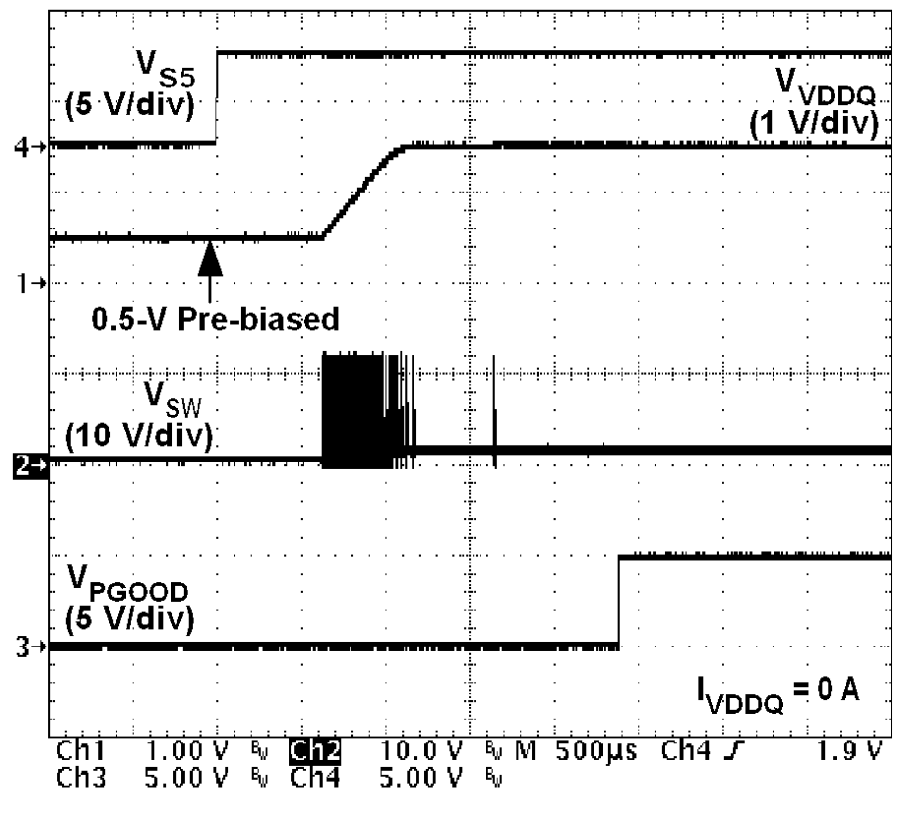 Figure 28. 1.5-V Startup Waveforms (0.5-V Pre-Biased)
 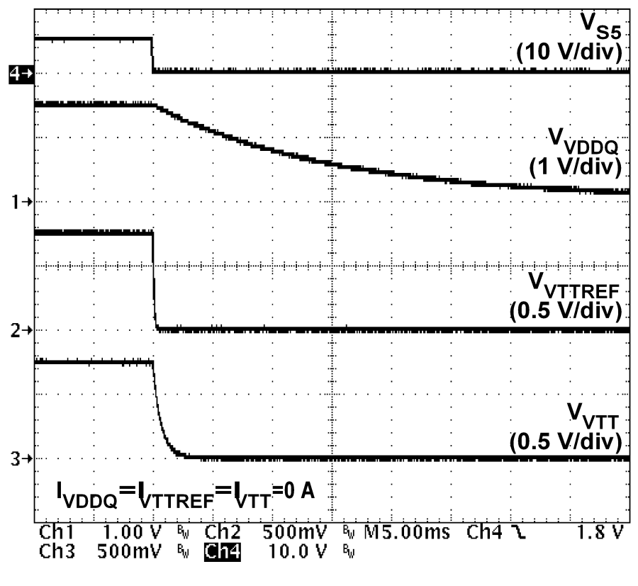 Figure 30. 1.5-V Soft-Stop Waveforms (Non-Tracking Discharge)
  Figure 32. VTT Bode Plot (Sink)