JAJSGZ5A May   2012  – February 2019 TPS53014

PRODUCTION DATA.  

  1. 特長
  2. アプリケーション
  3. 概要
    1.     Device Images
      1.      代表的なアプリケーション
  4. 改訂履歴
  5. Pin Configuration and Functions
    1.     Pin Functions
  6. Specifications
    1. 6.1 Absolute Maximum Ratings
    2. 6.2 Recommended Operating Conditions
    3. 6.3 Thermal Information
    4. 6.4 Electrical Characteristics
    5. 6.5 Typical Characteristics
  7. Detailed Description
    1. 7.1 Overview
    2. 7.2 Functional Block Diagram
    3. 7.3 Feature Description
      1. 7.3.1 PWM Operation
      2. 7.3.2 Auto-Skip Eco-Mode Control
      3. 7.3.3 Drivers
      4. 7.3.4 5-Volt Regulator
      5. 7.3.5 Soft Start and Pre-Biased Soft Start
      6. 7.3.6 Overcurrent Protection
      7. 7.3.7 Over/Undervoltage Protection
      8. 7.3.8 UVLO Protection
      9. 7.3.9 Thermal Shutdown
  8. Application and Implementation
    1. 8.1 Typical Application
      1. 8.1.1 Detailed Design Procedure
        1. 8.1.1.1 Component Selection
          1. 8.1.1.1.1 Inductor
          2. 8.1.1.1.2 Output Capacitor
          3. 8.1.1.1.3 Input Capacitor
          4. 8.1.1.1.4 Bootstrap Capacitor
          5. 8.1.1.1.5 VREG5 Capacitor
          6. 8.1.1.1.6 Choose Output Voltage Resistors
  9. Layout
    1. 9.1 Layout Guidelines
  10. 10デバイスおよびドキュメントのサポート
    1. 10.1 ドキュメントの更新通知を受け取る方法
    2. 10.2 コミュニティ・リソース
    3. 10.3 商標
    4. 10.4 静電気放電に関する注意事項
    5. 10.5 Glossary

パッケージ・オプション

メカニカル・データ(パッケージ|ピン)
サーマルパッド・メカニカル・データ
発注情報

Typical Application

A typical application schematic is shown in Figure 18.
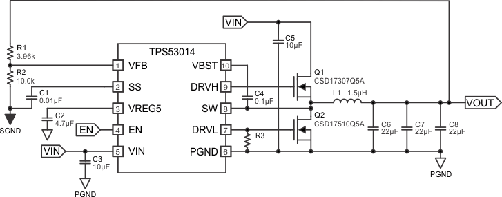
TPS53014 app_sch_slvsbf1.gifFigure 18. Application Schematic