SLUS909B May 2009 – August 2014 TPS53126
PRODUCTION DATA.
- 1 Features
- 2 Applications
- 3 Description
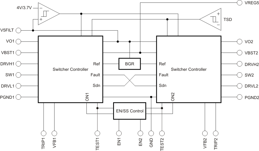
- 4 Simplified Schematics
- 5 Revision History
- 6 Pin Configurations and Functions
- 7 Specifications
-
8 Detailed Description
- 8.1 Overview
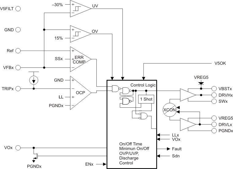
- 8.2 Functional Block Diagram
- 8.3
Feature Description
- 8.3.1 PWM Operation
- 8.3.2 Drivers
- 8.3.3 PWM Frequency And Adaptive On-time Control
- 8.3.4 5 Volt Regulator
- 8.3.5 Soft Start
- 8.3.6 Pre-Bias Support
- 8.3.7 Switching Frequency Selection
- 8.3.8 Output Discharge Control
- 8.3.9 Overcurrent Limit
- 8.3.10 Over/under Voltage Protection
- 8.3.11 UVLO Protection
- 8.3.12 Thermal Shutdown
- 8.4 Device Functional Modes
- 9 Application and Implementation
- 10Power Supply Recommendations
- 11Layout
- 12Device and Documentation Support
- 13Mechanical, Packaging, and Orderable Information
デバイスごとのパッケージ図は、PDF版データシートをご参照ください。
メカニカル・データ(パッケージ|ピン)
- RGE|24
- PW|24
サーマルパッド・メカニカル・データ
- RGE|24
8 Detailed Description
8.1 Overview
The TPS53126 is a dual, adaptive on-time, D-CAP2™ mode synchronous Buck controller. The TPS53126 enables system designers to complete the suite of various end equipment's power bus regulators with a cost effective, low external component count, and low standby current solution. The main control loop for the TPS53126 uses the D-CAP2™ mode control which provides a very fast transient response with no external components. The TPS53126 also has a proprietary circuit that enables the device to adapt to both low equivalent series resistance (ESR) output capacitors, such as POSCAP or SP-CAP, and ultra-low ESR ceramic capacitors. The device provides convenient and efficient operation with input voltages from 4.5 V to 24 V and output voltages from 0.76 V to 5.5 V.
8.2 Functional Block Diagram
8.3 Feature Description
8.3.1 PWM Operation
The main control loop of the TPS53126 is an adaptive on-time pulse width modulation (PWM) controller that supports a proprietary D-CAP2 mode control. D-CAP2 Mode control combines constant on-time control with an internal compensation circuit for pseudo-fixed frequency and low external component count configuration with both low ESR and ceramic output capacitors. It is stable even with virtually no ripple at the output.
At the beginning of each cycle, the high-side MOSFET is turned on. This MOSFET is turned off after internal one shot timer expires. This one shot timer is set by the converter input voltage ,VIN, and the output voltage ,VO, to maintain a pseudo-fixed frequency over the input voltage range, hence it is called adaptive on-time control. The one-shot timer is reset and the high-side MOSFET is turned on again when the feedback voltage falls below the reference voltage. An internal ramp is added to the reference voltage to simulate output ripple, eliminating the need for ESR induced output ripple from D-CAP mode control.
8.3.2 Drivers
Each SMPS of the TPS53126 contains 2 high-current resistive MOSFET drivers. The Low-side driver is a ground referenced, VREG5 powered driver designed to drive the gate of a high-current, low RDS(on) N-channel MOSFET whose source is connected to PGND. The High-side Driver is a floating SW referenced VBST powered driver designed to drive the gate of a high-current, low RDS(on) N-channel MOSFET. To maintain the BST voltage during the high-side driver ON time, a capacitor is placed from SW to VBST. Each driver draws average current equal to Gate Charge (Qg AT Vgs = 5V) times Switching Frequency (fsw).
To prevent cross-conduction, there is a narrow dead-time when both high-side and low-side drivers are OFF between each driver transition. During this time the inductor current is carried by one of the MOSFETs body diodes.
8.3.3 PWM Frequency And Adaptive On-time Control
The TPS53126 uses an adaptive on-time control scheme and does not have a dedicated on board oscillator. The TPS53126 runs with pseudo-constant frequency by using the input voltage and output voltage to set the on-time one-shot timer. The on-time is inversely proportional to the input voltage and proportional to the output voltage, therefore, when the duty ratio is VOUT/VIN, the frequency is constant.
8.3.4 5 Volt Regulator
The TPS53126 has an internal 5V Low-Dropout (LDO) Regulator to provide a regulated voltage for all four drivers and the ICs internal logic. A capacitor from VREG5 to GND is required to stabilize the internal regular. An internal 10Ω resistor from VREG5 filters the regulator output to the IC’s analog and logic input voltage, V5FILT. An additional capacitor is required from V5FILT to GND to filter switching noise from VREG5.
8.3.5 Soft Start
The TPS53126 has an internal, 1.2ms, voltage servo soft-start for each channel. When the ENx pin becomes high, an internal DAC begins ramping up the reference voltage to the PWM comparator. Smooth control of the output voltage is maintained during start up. As the TPS53126 shares one DAC with both channels, if ENx pin is set to high while another channel is starting up, soft start is postponed until another channel soft start has completed. If both of EN1 and EN2 are set high at a same time, both channels start up at same time.
8.3.6 Pre-Bias Support
The TPS53126 supports pre-bias start-up without sinking current from the output capacitor. When enabled, the low-side driver is held off until the soft-start commands a voltage higher than the pre-bias level (internal soft-start becomes greater than feedback voltage [VFB]), then the TPS53126 slowly activates synchronous rectification by limiting the first DRVL pulses with a narrow on-time. This limited on-time is then incremented on a cycle-by-cycle basis until it coincides with the full 1-D off-time. This scheme prevents the initial sinking of current from the pre-bias output, and ensure that the output voltage (VOUT) starts and ramps up smoothly into regulation and the control loop is given time to transition from pre-biased start-up to normal mode operation.
8.3.7 Switching Frequency Selection
The TPS53126 allows the user to select from 2 different switching frequencies by connecting the TEST2 pin to either GND or V5FILT. Connect TEST2 to GND for a switching frequency (fsw) of 350KHz. Connect TEST2 to V5FILT for a switching frequency of 700KHz.
8.3.8 Output Discharge Control
The TPS53126 discharges the outputs when ENx is low, or when the controller is turned off by the protection functions (OVP, UVP, UVLO, and thermal shutdown). The device discharges an output using an internal 40-Ω MOSFET which is connected to VOx and PGNDx. The external low-side MOSFET is not turned on during the output discharge operation to avoid the possibility of causing negative voltage at the output. This discharge ensures that, on start, the regulated voltage always initializes from zero volts.
8.3.9 Overcurrent Limit
The TPS53126 has a cycle-by-cycle over current limit feature. The over current limits the inductor valley current by monitoring the voltage drop across the low-side MOSFET RDS(on) during the low-side driver on-time. If the inductor current is larger than the over current limit (OCL), the TPS53126 delays the start of the next switching cycle until the sensed inductor current falls below the OCL current. MOSFET RDS(on) current sensing is used to provide an accuracy and cost effective solution without external devices. To program the OCL, the TRIPx pin should be connected to GND through a trip voltage setting resistor, according to the following equations.
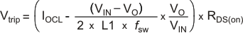
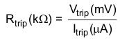
The trip voltage should be between 30mV to 300mV over all operational temperature, including the 4000ppm/°C temperature slope compensation for the temperature dependency of the RDS(on). If the load current exceeds the over-current limit, the voltage will begin to drop. If the over-current conditions continues the output voltage will fall below the under voltage protection threshold and the TPS53126 will shut down.
8.3.10 Over/under Voltage Protection
The TPS53126 monitors the output voltage via the feedback voltage to detect over and under voltage. When the feedback voltage becomes higher than 115% of the reference voltage, the TPS53126 turns off the high-side MOSFET driver, turns on the low-side MOSFET driver and latches off.
When the feedback voltage becomes lower than 70% of the reference voltage, the TPS53126 begins an internal UVP delay counter. After 30μs, the TPS53126 turns off both top and bottom MOSFET drivers and latches off. The UVP function is enabled approximately 2.0ms after power-on to prevent detecting UVP during soft-start. Both OVP and UVP latch conditions are reset when V5FILT triggers UVLO or the ENx pin goes low.
8.3.11 UVLO Protection
The TPS53126 has under voltage lock out protection (UVLO) that monitors the voltage of V5FILT pin. When the V5FILT voltage is lower than UVLO threshold voltage, the device is shut off. During shut-off, VREG5 and all output drivers are OFF and output discharge is ON. The UVLO is non-latch protection.
8.3.12 Thermal Shutdown
The TPS53126 includes an over temperature protection shut-down feature. If the TPS53126 die temperature exceeds the OTP threshold (typically 150°C), both the high-side and low-side drivers are shut off, the output voltage discharge function is enabled and then the device is shut off until the die temperature drops. Thermal shutdown is a non-latch protection.
8.4 Device Functional Modes
The TPS53126 has two operating modes. The TPS53126 is in shut down mode when the EN1 and EN2 pins are low. When the EN1 and EN2 pins is pulled high, the TPS53126 enters the normal operating mode.