JAJS531A December   2010  – November 2016 TPS53321

PRODUCTION DATA.  

  1. 特長
  2. アプリケーション
  3. 概要
  4. 改訂履歴
  5. Pin Configuration and Functions
  6. Specifications
    1. 6.1 Absolute Maximum Ratings
    2. 6.2 ESD Ratings
    3. 6.3 Recommended Operating Conditions
    4. 6.4 Thermal Information
    5. 6.5 Electrical Characteristics
    6. 6.6 Typical Characteristics
  7. Detailed Description
    1. 7.1 Overview
    2. 7.2 Functional Block Diagram
    3. 7.3 Feature Description
      1. 7.3.1 Soft Start
      2. 7.3.2 Power Good
      3. 7.3.3 Undervoltage Lockout (UVLO) Protection
      4. 7.3.4 Overcurrent Protection
      5. 7.3.5 Overvoltage Protection
      6. 7.3.6 Undervoltage Protection
      7. 7.3.7 Overtemperature Protection
      8. 7.3.8 Output Discharge
      9. 7.3.9 Master and Slave Operation and Synchronization
    4. 7.4 Device Functional Modes
      1. 7.4.1 Operation Modes
      2. 7.4.2 Eco-Mode™ Light-Load Operation
      3. 7.4.3 Forced Continuous Conduction Mode (FCCM)
  8. Application and Implementation
    1. 8.1 Application Information
    2. 8.2 Typical Application
      1. 8.2.1 Design Requirements
      2. 8.2.2 Detailed Design Procedure
        1. 8.2.2.1 Determine the Value of R1 and R2
        2. 8.2.2.2 Choose the Inductor
        3. 8.2.2.3 Choose the Output Capacitor(s)
        4. 8.2.2.4 Choose the Input Capacitor
        5. 8.2.2.5 Compensation Design
      3. 8.2.3 Application Curves
  9. Power Supply Recommendations
  10. 10Layout
    1. 10.1 Layout Guidelines
    2. 10.2 Layout Example
  11. 11デバイスおよびドキュメントのサポート
    1. 11.1 ドキュメントの更新通知を受け取る方法
    2. 11.2 コミュニティ・リソース
    3. 11.3 商標
    4. 11.4 静電気放電に関する注意事項
    5. 11.5 Glossary
  12. 12メカニカル、パッケージ、および注文情報

パッケージ・オプション

メカニカル・データ(パッケージ|ピン)
サーマルパッド・メカニカル・データ
発注情報

Layout

Layout Guidelines

Good layout is essential for stable power supply operation. Follow these guidelines for a clean PCB layout:

  • Separate the power ground and analog ground planes. Connect them together at one location.
  • Use four vias to connect the thermal pad to power ground.
  • Place VIN and VDD decoupling capacitors as close to the device as possible.
  • Use wide traces for VIN, VOUT, PGND, and SW. These nodes carry high current and also serve as heat sinks.
  • Place feedback and compensation components as close to the device as possible.
  • Keep analog signals (FB, COMP) away from noisy signals (SW, SYNC, VBST).
  • See TPS53321 evaluation module for a layout example.

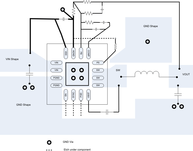
Figure 26 shows and example layout for the TPS53321.

Layout Example

TPS53321 v10214_lusaf3.gif Figure 26. TPS53321 Layout Example