JAJS531A December 2010 – November 2016 TPS53321
PRODUCTION DATA.
- 1 特長
- 2 アプリケーション
- 3 概要
- 4 改訂履歴
- 5 Pin Configuration and Functions
- 6 Specifications
- 7 Detailed Description
- 8 Application and Implementation
- 9 Power Supply Recommendations
- 10Layout
- 11デバイスおよびドキュメントのサポート
- 12メカニカル、パッケージ、および注文情報
パッケージ・オプション
メカニカル・データ(パッケージ|ピン)
- RGT|16
サーマルパッド・メカニカル・データ
- RGT|16
発注情報
6 Specifications
6.1 Absolute Maximum Ratings
over operating free-air temperature range (unless otherwise noted)(1)| MIN | MAX | UNIT | |||
|---|---|---|---|---|---|
| Input voltage | VIN, EN | –0.3 | 7 | V | |
| VBST | –0.3 | 17 | |||
| VBST(with respect to SW) | –0.3 | 7 | |||
| FB, PS, VDD | –0.3 | 3.7 | |||
| Output voltage | SW | DC | –0.3 | 7 | V |
| Pulse < 20 ns, E = 5 µJ | –3 | 10 | |||
| PGD | –0.3 | 7 | |||
| COMP, SYNC | –0.3 | 3.7 | |||
| PGND | –0.3 | 0.3 | |||
| Junction temperature, TJ | –40 | 150 | °C | ||
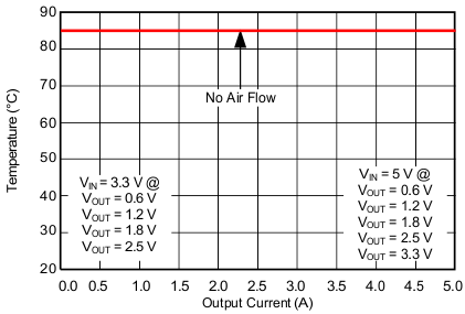
| Ambient temperature, TA | –40 | 85 | °C | ||
| Storage temperature, Tstg | –55 | 150 | °C | ||
(1) Stresses beyond those listed under Absolute Maximum Ratings may cause permanent damage to the device. These are stress ratings only, which do not imply functional operation of the device at these or any other conditions beyond those indicated under Recommended Operating Conditions. Exposure to absolute-maximum-rated conditions for extended periods may affect device reliability.
6.2 ESD Ratings
| VALUE | UNIT | |||
|---|---|---|---|---|
| V(ESD) | Electrostatic discharge | Human-body model (HBM), per ANSI/ESDA/JEDEC JS-001(1) | ±2000 | V |
| Charged-device model (CDM), per JEDEC specification JESD22-C101(2) | ±500 | |||
(1) JEDEC document JEP155 states that 500-V HBM allows safe manufacturing with a standard ESD control process.
(2) JEDEC document JEP157 states that 250-V CDM allows safe manufacturing with a standard ESD control process.
6.3 Recommended Operating Conditions
| MIN | NOM | MAX | UNIT | |||
|---|---|---|---|---|---|---|
| Input voltage | VIN | 2.9 | 6 | V | ||
| VDD | 2.9 | 3.3 | 3.5 | |||
| VBST | –0.1 | 13.5 | ||||
| VBST(with respect to SW) | –0.1 | 6 | ||||
| EN | –0.1 | 6 | ||||
| FB, PS | –0.1 | 3.5 | ||||
| Output voltage | SW | –1 | 6.5 | V | ||
| PGD | –0.1 | 6 | ||||
| COMP, SYNC | –0.1 | 3.5 | ||||
| PGND | –0.1 | 0.1 | ||||
| TJ | Junction temperature | –40 | 125 | °C | ||
6.4 Thermal Information
| THERMAL METRIC(1) | TPS53321 | UNIT | |
|---|---|---|---|
| RGT (QFN) | |||
| 16 PINS | |||
| RθJA | Junction-to-ambient thermal resistance | 42.8 | °C/W |
| RθJC(top) | Junction-to-case (top) thermal resistance | 51.3 | °C/W |
| RθJB | Junction-to-board thermal resistance | 16 | °C/W |
| ψJT | Junction-to-top characterization parameter | 0.7 | °C/W |
| ψJB | Junction-to-board characterization parameter | 16 | °C/W |
| RθJC(bot) | Junction-to-case (bottom) thermal resistance | 4.4 | °C/W |
(1) For more information about traditional and new thermal metrics, see the Semiconductor and IC Package Thermal Metrics application report.
6.5 Electrical Characteristics
over recommended free-air temperature range, VIN = 3.3 V, VVDD = 3.3 V, and PGND = GND (unless otherwise noted)| PARAMETER | TEST CONDITIONS | MIN | TYP | MAX | UNIT | |
|---|---|---|---|---|---|---|
| SUPPLY: VOLTAGE, CURRENTS, and UVLO | ||||||
| VIN | VIN supply voltage | Nominal input voltage range | 2.9 | 6 | V | |
| IVINSDN | VIN shutdown current | EN = LO | 3 | µA | ||
| VUVLO | VIN UVLO threshold | Ramp up, EN = HI | 2.8 | V | ||
| VUVLOHYS | VIN UVLO hysteresis | VIN UVLO Hysteresis | 130 | mV | ||
| VDD | Internal circuitry supply voltage | Nominal 3.3-V input voltage range | 2.9 | 3.3 | 3.5 | V |
| IDDSDN | VDD shutdown current | EN = LO | 5 | µA | ||
| IDD | Standby current | EN = HI, no switching | 2.2 | 3.5 | mA | |
| VDDUVLO | 3.3-V UVLO threshold | Ramp up, EN = HI | 2.8 | V | ||
| VDDUVLOHYS | 3.3-V UVLO hysteresis | 75 | mV | |||
| VOLTAGE FEEDBACK LOOP: VREF AND ERROR AMPLIFIER | ||||||
| VVREF | VREF | Internal precision reference voltage | 0.6 | V | ||
| TOLVREF | VREF Tolerance | 0°C ≤ TA ≤ 85°C | –1% | 1% | ||
| –40°C ≤ TA ≤ 85°C | –1.25% | 1.25% | ||||
| UGBW(1) | Unity gain bandwidth | 14 | MHz | |||
| AOL(1) | Open-loop gain | 80 | dB | |||
| IFBINT | FB input leakage current | Sourced from FB pin | 30 | nA | ||
| IEAMAX(1) | Output sinking and sourcing current | CCOMP = 20 pF | 5 | mA | ||
| SR(1) | Slew rate | 5 | V/µs | |||
| OCP: OVERCURRENT AND ZERO CROSSING | ||||||
| IOCPL | Overcurrent limit on upper FET | When IOUT exceeds this threshold for 4 consecutive cycles. VIN=3.3 V, VOUT=1.5 V with 1-µH inductor, TA = 25°C |
6 | 6.5 | 7 | A |
| IOCPH | One time overcurrent latch off on the lower FET | Immediately shuts down when sensed current reach this value. VIN=3.3 V, VOUT=1.5 V with 1-µH inductor, TA = 25°C |
6.25 | 6.8 | 7.35 | A |
| tHICCUP | Hiccup time interval | 12.5 | 14.5 | 16.5 | ms | |
| VZXOFF(1) | Zero crossing comparator internal offset | PGND – SW, skip mode | –4.5 | –3 | –1.5 | mV |
| PROTECTION: OVP, UVP, PGD, AND INTERNAL THERMAL SHUTDOWN | ||||||
| VOVP | Overvoltage protection threshold voltage | Measured at FB w/r/t VREF | 114% | 117% | 120% | |
| VUVP | Undervoltage protection threshold voltage | Measured at FB w/r/t VREF | 80% | 83% | 86% | |
| VPGDL | PGD low threshold | Measured at FB w/r/t VREF | 80% | 83% | 86% | |
| VPGDU | PGD upper threshold | Measured at FB w/r/t VREF | 114% | 117% | 120% | |
| VINMINPG | Minimum Vin voltage for valid PGD at start-up | Measured at VIN with 1-mA (or 2-mA) sink current on PGD pin at start-up | 1 | V | ||
| THSD(1) | Thermal shutdown | Latch off controller, attempt soft-stop | 130 | 140 | 150 | °C |
| THSDHYS(1) | Thermal shutdown hysteresis | Controller restarts after temperature has dropped | 40 | °C | ||
| LOGIC PINS: I/O VOLTAGE AND CURRENT | ||||||
| VPGPD | PGD pulldown voltage | Pulldown voltage with 4-mA sink current | 0.2 | 0.4 | V | |
| IPGLK | PGD leakage current | Hi-Z leakage current, apply 3.3-V in off state | –2 | 0 | 2 | µA |
| RENPU | Enable pullup resistor | 1.35 | MΩ | |||
| VENH | EN logic high threshold | 1.1 | 1.18 | 1.3 | V | |
| VENHYS | EN hysteresis | 0.18 | 0.24 | V | ||
| PSTHS | PS mode threshold voltage | Level 1 to level 2(2) | 0.12 | V | ||
| Level 2 to level 3 | 0.4 | |||||
| Level 3 to level 4 | 0.8 | |||||
| Level 4 to level 5 | 1.4 | |||||
| Level 5 to level 6 | 2.2 | |||||
| IPS | PS source | 10-µA pullup current when enabled | 8 | 10 | 12 | µA |
| fSYNCSL | Slave SYNC frequency range | Versus nominal switching frequency | –20% | 20% | ||
| PWSYNC | SYNC low pulse width | 110 | ns | |||
| ISYNC | SYNC pin sink current | TA = 25°C | 10 | µA | ||
| VSYNCTHS(1) | SYNC threshold | Falling edge | 1 | V | ||
| VSYNCHYS(1) | SYNC hysteresis | 0.5 | V | |||
| BOOT STRAP: VOLTAGE AND LEAKAGE CURRENT | ||||||
| IVBSTLK | VBST leakage current | VIN = 3.3 V, VVBST = 6.6 V, TA = 25°C | 1 | µA | ||
| TIMERS: SS, FREQUENCY, RAMP, ON-TIME AND I/O TIMING | ||||||
| tSS_1 | Delay after EN asserting | EN = HI, master or HEF mode | 0.2 | ms | ||
| tSS_2 | Delay after EN asserting | EN = HI, slave waiting time | 0.5 | ms | ||
| tSS_3 | Soft-start ramp-up time | Rising from VSS = 0 V to VSS = 0.6 V | 0.4 | ms | ||
| tPGDENDLY | PGD start-up delay time | Rising from VSS = 0 V to VSS = 0.6 V, from VSS reaching 0.6 V to VPGD going high |
1.2 | ms | ||
| tOVPDLY | Overvoltage protection delay time | Time from FB out of +20% of VREF to OVP fault | 1 | 1.7 | 2.5 | µs |
| tUVPDLY | Undervoltage protection delay time | Time from FB out of –20% of VREF to UVP fault | 11 | µs | ||
| fSW | Switching frequency control | FCCM | 0.99 | 1.1 | 1.21 | MHz |
| Ramp amplitude(1) | 2.9 V < VIN < 6.0 V | VIN/4 | V | |||
| tMIN(off) | Minimum OFF time | FCCM or DE mode | 100 | 140 | ns | |
| HEF mode | 175 | 250 | ||||
| DMAX | Maximum duty cycle, FCCM and DE mode | fSW = 1.1 MHz, 0°C ≤ TA ≤ 85°C | 84% | 89% | ||
| Maximum duty cycle, HEF mode | fSW = 1.1 MHz, 0°C ≤ TA ≤ 85°C | 75% | 81% | |||
| RSFTSTP | Soft-discharge transistor resistance | VEN = Low, VIN = 3.3 V, VOUT = 0.5 V | 60 | Ω | ||
(1) Ensured by design. Not production tested.
(2) See PS pin description for levels.
6.6 Typical Characteristics
Inductor PCMC065T-1R0 (1 µH, 5.6 mΩ) is used.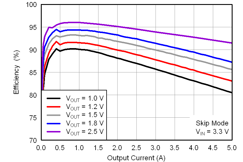 Figure 1. Efficiency vs Output Current,
Skip Mode, VIN = 3.3 V
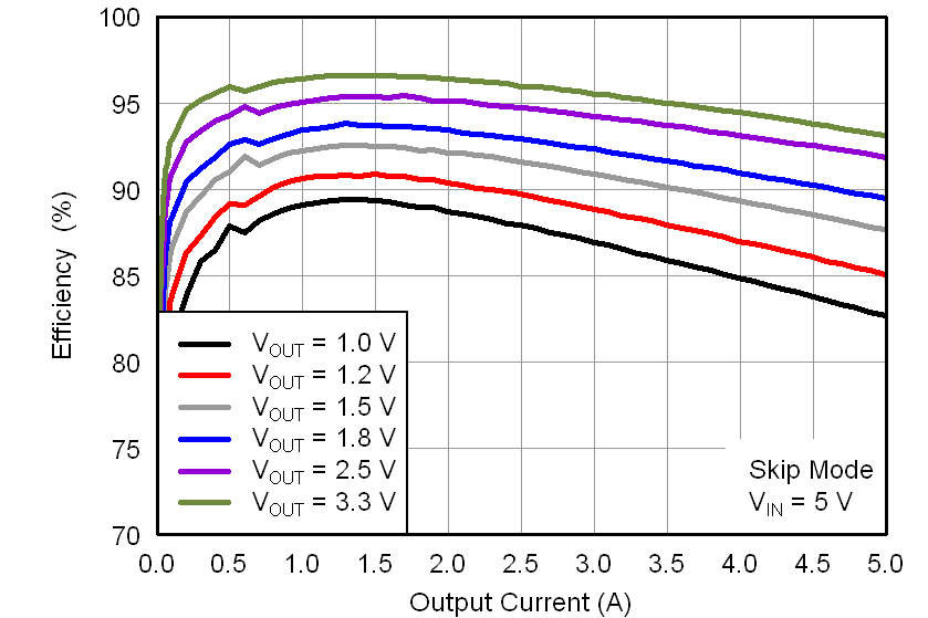 Figure 3. Efficiency vs Output Current,
Skip Mode, VIN = 5 V
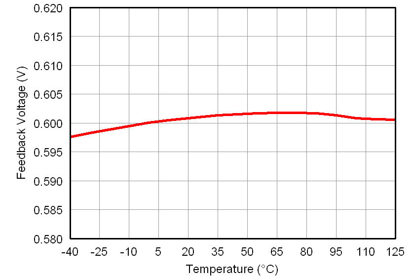 Figure 5. Feedback Voltage vs Ambient Temperature
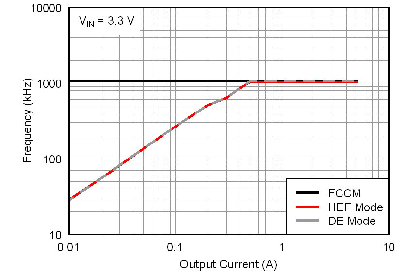 Figure 7. Frequency vs Output Current
at VIN = 3.3 V
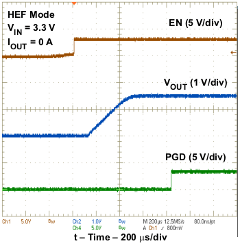 Figure 9. Normal Start-Up Waveform
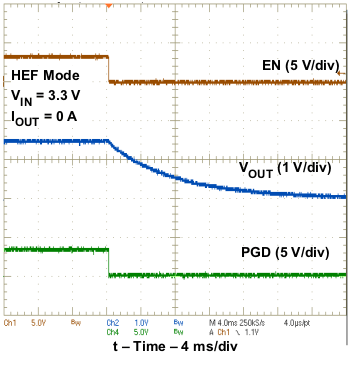 Figure 11. Soft-Stop Waveform
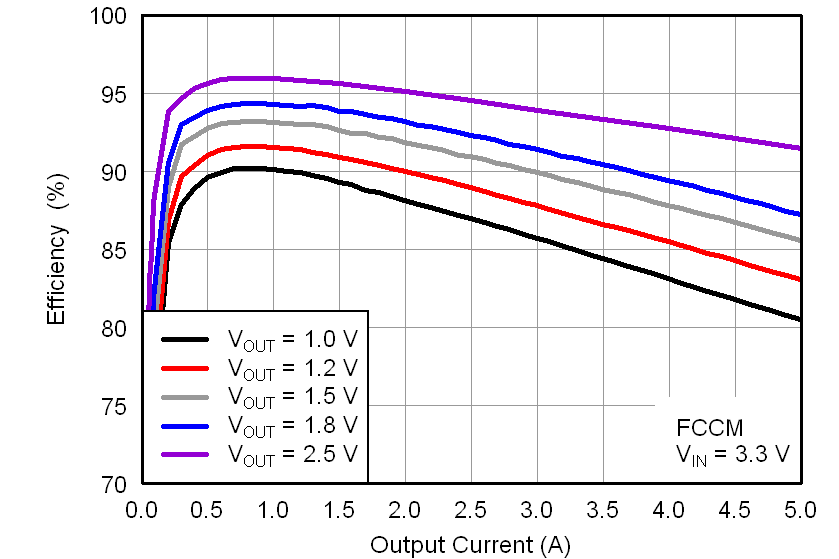 Figure 2. Efficiency vs Output Current,
FCCM, VIN = 3.3 V
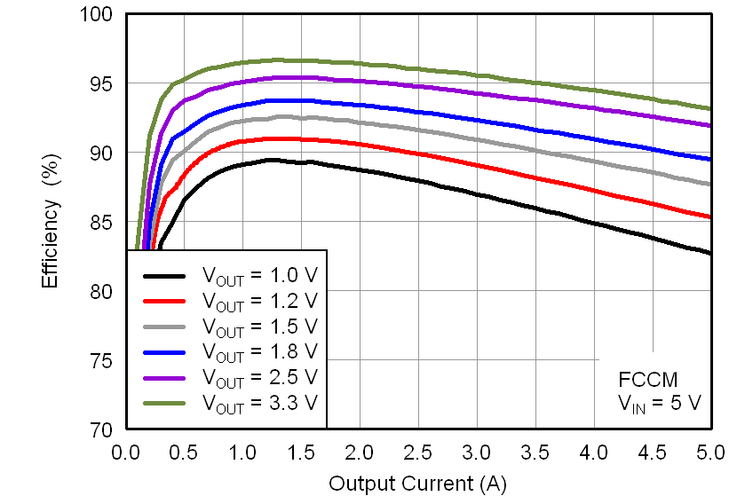 Figure 4. Efficiency vs Output Current,
FCCM, VIN = 5 V
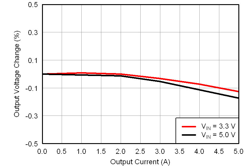 Figure 6. Output Voltage Change vs Output Current
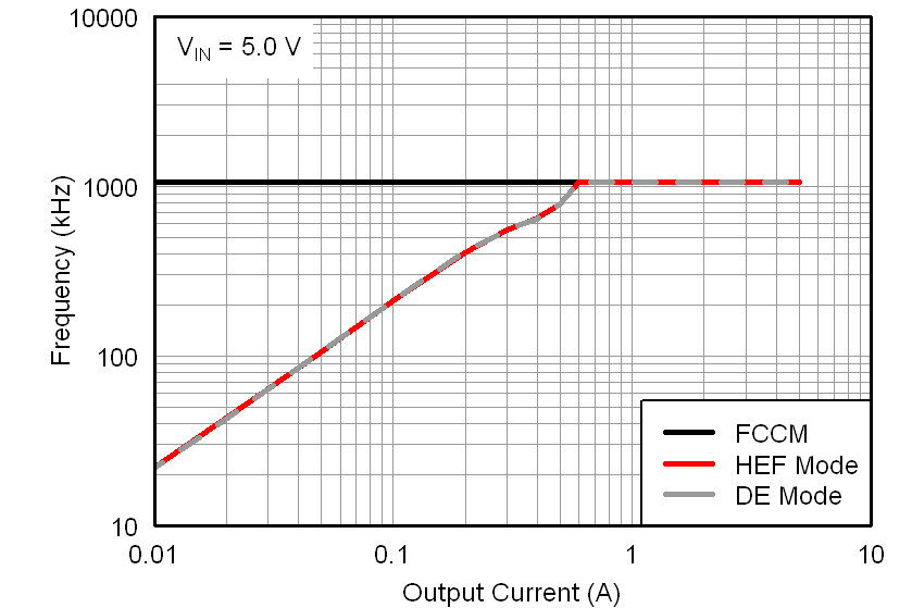 Figure 8. Frequency vs Output Current
at VIN = 5 V
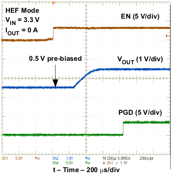 Figure 10. Prebias Start-Up Waveform
