JAJSML7B March   2013  – August 2021 TPS53511

PRODUCTION DATA  

  1. 特長
  2. アプリケーション
  3. 概要
  4. Revision History
  5. Pin Configuration and Functions
  6. Specifications
    1. 6.1 Absolute Maximum Ratings
    2. 6.2 ESD Ratings
    3. 6.3 Recommended Operating Conditions
    4. 6.4 Thermal Information
    5. 6.5 Electrical Characteristics
    6. 6.6 Typical Characteristics
  7. Detailed Description
    1. 7.1 Overview
    2. 7.2 Functional Block Diagram
    3. 7.3 Feature Description
      1. 7.3.1 PWM Operation
      2. 7.3.2 PWM Frequency and Adaptive On-Time Control
      3. 7.3.3 Soft Start and Pre-Biased Soft-Start Function
      4. 7.3.4 Power Good
      5. 7.3.5 Output Discharge Control
      6. 7.3.6 Current Protection
      7. 7.3.7 Overvoltage/Undervoltage Protection
      8. 7.3.8 UVLO Protection
      9. 7.3.9 Thermal Shutdown
    4. 7.4 Device Functional Modes
      1. 7.4.1 Light Load Mode Control
  8. Application and Implementation
    1. 8.1 Application Information
    2. 8.2 Typical Application
      1. 8.2.1 Design Requirements
      2. 8.2.2 Detailed Design Procedure
        1. 8.2.2.1 Output Inductor Selection
        2. 8.2.2.2 Output Capacitor Selection
        3. 8.2.2.3 Input Capacitor Selection
        4. 8.2.2.4 Bootstrap Capacitor Selection
        5. 8.2.2.5 VREG5 Capacitor Selection
        6. 8.2.2.6 Output Voltage Setting Resistors Selection
      3. 8.2.3 Application Curves
  9. Power Supply Recommendations
  10. 10Layout
    1. 10.1 Layout Considerations
      1. 10.1.1 Thermal Information
    2. 10.2 Layout Example
  11. 11Device and Documentation Support
    1. 11.1 Device Support
      1. 11.1.1 Third-Party Products Disclaimer
    2. 11.2 Receiving Notification of Documentation Updates
    3. 11.3 サポート・リソース
    4. 11.4 Trademarks
    5. 11.5 Electrostatic Discharge Caution
    6. 11.6 Glossary
  12. 12Mechanical, Packaging, and Orderable Information

パッケージ・オプション

メカニカル・データ(パッケージ|ピン)
サーマルパッド・メカニカル・データ
発注情報

Typical Characteristics

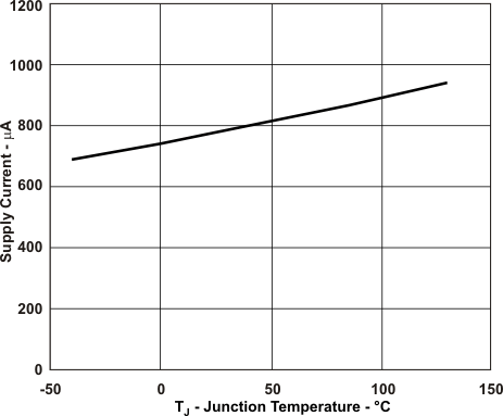
GUID-1D10CC64-091F-4B84-B315-5D93851BB9E6-low.gifFigure 6-1 VCC Supply Current vs. Junction Temperature
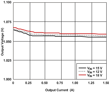
GUID-F3FA4C79-23CD-4B20-AE66-47E86CA5CB66-low.gifFigure 6-3 1.05-V Output Voltage vs. Output Current
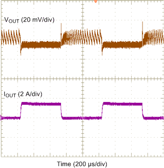
GUID-D7E1382B-14CC-4A86-BC7E-A90C4233AD14-low.gifFigure 6-5 Load Transient Response, 1.05 V, 0 A to 1.5 A
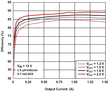
GUID-67A47371-1AF3-40E3-A678-95C61E8135A7-low.gifFigure 6-7 Efficiency vs. Output Current
GUID-B11FCD6A-158D-4FD9-8F52-E91567C0EF5C-low.gifFigure 6-9 Switching Frequency vs Input Voltage
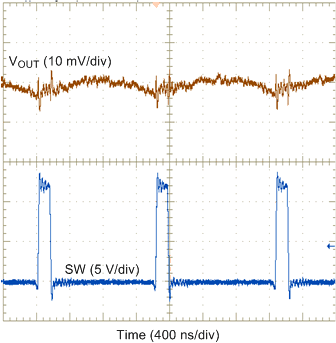
GUID-F5D2F3CA-08E0-441F-AC41-6F1C1452AB11-low.gifFigure 6-11 Output Voltage Ripple
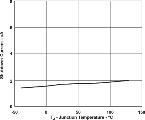
GUID-D3B84DD3-434D-477A-82DD-8F7995C8B220-low.gifFigure 6-2 VCC Shutdown Current vs. Junction Temperature
GUID-297275EF-6E14-45C2-B591-B15FB3F685E9-low.gifFigure 6-4 1.05-V Output Voltage vs. Input Voltage
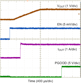
GUID-51466FC4-C393-43B9-91B5-57DBC9B19A01-low.gifFigure 6-6 Start-Up
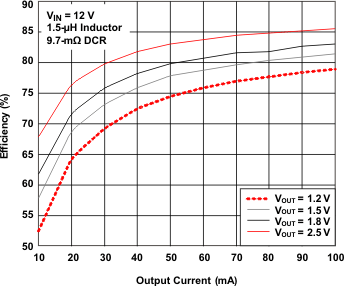
GUID-E5781B64-9D7B-4B46-8E73-62E198F5FDBA-low.gifFigure 6-8 Light Load Efficiency vs. Output Current
GUID-20548C20-EB47-4012-9C60-D4EA3A089D5C-low.gifFigure 6-10 Switching Frequency vs Output Current
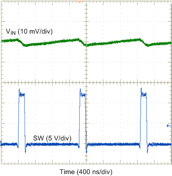
GUID-445E3516-99A8-440E-9B93-6AED8C820A51-low.gifFigure 6-12 Input Voltage Ripple