JAJS249E August 2006 – January 2024 TPS5410
PRODUCTION DATA
- 1
- 1 特長
- 2 アプリケーション
- 3 概要
- 4 Pin Configuration and Functions
- 5 Specifications
-
6 Detailed Description
- 6.1 Overview
- 6.2 Functional Block Diagram
- 6.3
Feature Description
- 6.3.1 Oscillator Frequency
- 6.3.2 Voltage Reference
- 6.3.3 Enable (ENA) and Internal Slow-Start
- 6.3.4 Undervoltage Lockout (UVLO)
- 6.3.5 Boost Capacitor (BOOT)
- 6.3.6 Output Feedback (VSENSE)
- 6.3.7 Internal Compensation
- 6.3.8 Voltage Feed-Forward
- 6.3.9 Pulse-Width-Modulation (PWM) Control
- 6.3.10 Overcurrent Limiting
- 6.3.11 Overvoltage Protection
- 6.3.12 Thermal Shutdown
- 6.4 Device Functional Modes
-
7 Applications and Implementation
- 7.1 Application Information
- 7.2
Typical Applications
- 7.2.1 Application Circuit
- 7.2.2 Using All Ceramic Capacitors
- 7.3 Power Supply Recommendations
- 7.4 Layout
- 8 Device and Documentation Support
- 9 Revision History
- 10Mechanical, Packaging, and Orderable Information
7.2.1.3 Application Curves
The performance graphs in Figure 7-2 to Figure 7-9 are applicable to the circuit in Figure 7-1. TA = 25 °C. unless otherwise specified.
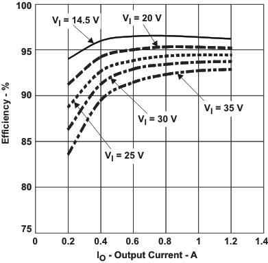 Figure 7-2 Efficiency vs Output Current
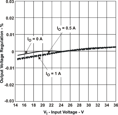 Figure 7-4 Output Voltage Regulation % vs Input Voltage
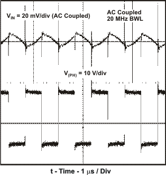 Figure 7-6 Output Voltage Ripple and PH Node, IO = 1 A
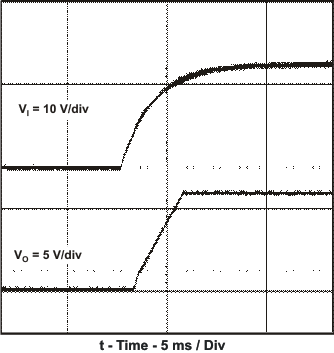 Figure 7-8 Start-up Waveform, VI and VO
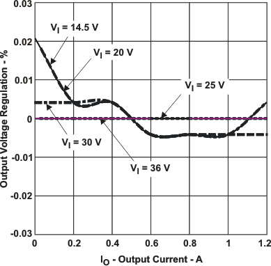 Figure 7-3 Output Voltage Regulation % vs Output Current
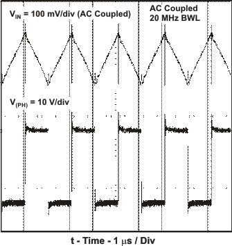 Figure 7-5 Input
Voltage Ripple and PH Node, IO = 1 A
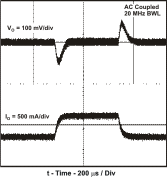 Figure 7-7 Transient Response, IO Step 0.25 to 0.75 A
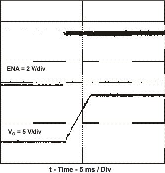 Figure 7-9 Start-up Waveform, ENA and VO