JAJSCQ2B November   2016  – June 2018 TPS54200 , TPS54201

PRODUCTION DATA.  

  1. 特長
  2. アプリケーション
  3. 概要
    1.     Device Images
      1.      概略回路図
      2.      ADIMでの優れた深調光機能
  4. 改訂履歴
  5. 概要(続き)
  6. Pin Configuration and Functions
    1.     Pin Functions
  7. Specifications
    1. 7.1 Absolute Maximum Ratings
    2. 7.2 ESD Ratings
    3. 7.3 Recommended Operating Conditions
    4. 7.4 Thermal Information
    5. 7.5 Electrical Characteristics
    6. 7.6 Timing Requirements
    7. 7.7 Switching Characteristics
    8. 7.8 Typical Characteristics
  8. Detailed Description
    1. 8.1 Overview
    2. 8.2 Functional Block Diagram
    3. 8.3 Feature Description
      1. 8.3.1  Fixed-Frequency PWM Control
      2. 8.3.2  Error Amplifier
      3. 8.3.3  Slope Compensation and Output Current
      4. 8.3.4  Input Undervoltage Lockout
      5. 8.3.5  Voltage Reference
      6. 8.3.6  Setting LED Current
      7. 8.3.7  Internal Soft Start
      8. 8.3.8  Bootstrap Voltage (BOOT)
      9. 8.3.9  Overcurrent Protection
        1. 8.3.9.1 High-Side MOSFET Overcurrent Protection
        2. 8.3.9.2 Low-Side MOSFET Overcurrent Protection
        3. 8.3.9.3 Low-Side MOSFET Reverse Overcurrent Protection
      10. 8.3.10 Fault Protection
        1. 8.3.10.1 LED-Open Protection
        2. 8.3.10.2 LED Short Protection
        3. 8.3.10.3 Sense-Resistor Short Protection
        4. 8.3.10.4 Sense-Resistor Open Protection
        5. 8.3.10.5 Overvoltage Protection
        6. 8.3.10.6 Thermal Shutdown
    4. 8.4 Device Functional Modes
      1. 8.4.1 Enable and Disable Device
      2. 8.4.2 Mode Detection
      3. 8.4.3 Analog Dimming Mode Operation
      4. 8.4.4 PWM Dimming-Mode Operation
  9. Application and Implementation
    1. 9.1 Application Information
    2. 9.2 Typical Application
      1. 9.2.1 TPS5420x 12-V Input, 1.5-A, 3-Piece IR LED Driver With Analog Dimming
        1. 9.2.1.1 Design Requirements
        2. 9.2.1.2 Detailed Design Procedure
          1. 9.2.1.2.1 Inductor Selection
          2. 9.2.1.2.2 Input Capacitor Selection
          3. 9.2.1.2.3 Output Capacitor Selection
          4. 9.2.1.2.4 FB Pin RC Filter Selection
          5. 9.2.1.2.5 Sense Resistor Selection
        3. 9.2.1.3 Application Curves
      2. 9.2.2 TPS5420x 24-V Input, 1-A, 4-Piece WLED Driver With PWM Dimming
        1. 9.2.2.1 Design Requirements
        2. 9.2.2.2 Detailed Design Procedure
          1. 9.2.2.2.1 Inductor Selection
          2. 9.2.2.2.2 Input Capacitor Selection
          3. 9.2.2.2.3 Output Capacitor Selection
          4. 9.2.2.2.4 FB Pin RC Filter Selection
          5. 9.2.2.2.5 Sense Resistor Selection
        3. 9.2.2.3 Application Curves
  10. 10Power Supply Recommendations
  11. 11Layout
    1. 11.1 Layout Guidelines
    2. 11.2 Layout Example
  12. 12デバイスおよびドキュメントのサポート
    1. 12.1 デバイス・サポート
      1. 12.1.1 デベロッパー・ネットワークの製品に関する免責事項
    2. 12.2 ドキュメントのサポート
      1. 12.2.1 関連リンク
    3. 12.3 ドキュメントの更新通知を受け取る方法
    4. 12.4 コミュニティ・リソース
    5. 12.5 商標
    6. 12.6 静電気放電に関する注意事項
    7. 12.7 Glossary
  13. 13メカニカル、パッケージ、および注文情報

パッケージ・オプション

メカニカル・データ(パッケージ|ピン)
サーマルパッド・メカニカル・データ
発注情報

PWM Dimming-Mode Operation

Once the PWM dimming mode is chosen, the internal voltage reference for the FB pin is fixed at 100 mV. The LED current is on or off corresponding to the PWM state, see Figure 19. Due to the limited control-loop response, to get a relatively linear dimming performance, the suggested PWM signal frequency should be less than 1 kHz.
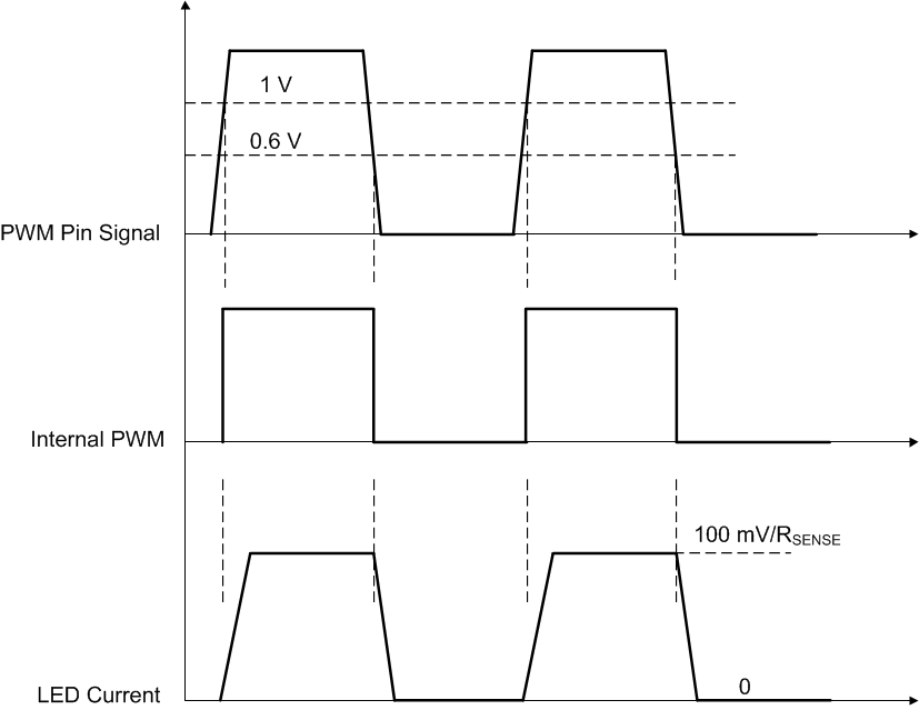
TPS54200 TPS54201 dimop2_lusco8.gifFigure 19. PWM Dimming Operation

In some application where dimming is not needed, one can just connect a resistor divider from VVIN to the PWM pin as Figure 20 shows.
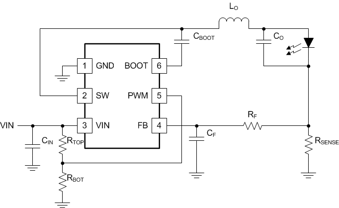
TPS54200 TPS54201 wodim_lusco8.gifFigure 20. Application Without Dimming

RTOP and RBOT should be sized to make sure the PWM pin voltage is higher than 1 V when VVIN reaches its steady voltage. It is best to make sure the PWM pin voltage is less than 2 V, thus one can have 100 mV at the FB pin for better efficiency. Use 10 kΩ as a good starting point for RBOT, then choose RTOP according to Equation 2:

Equation 2. TPS54200 TPS54201 qu2_lusco8.gif