JAJSDK1B May 2017 – March 2018 TPS543B20
PRODUCTION DATA.
- 1 特長
- 2 アプリケーション
- 3 概要
- 4 改訂履歴
- 5 Device Comparison Table
- 6 Pin Configuration and Functions
- 7 Specifications
-
8 Detailed Description
- 8.1 Overview
- 8.2 Functional Block Diagram
- 8.3 Feature Description
- 8.4
Device Functional Modes
- 8.4.1 Soft-Start Operation
- 8.4.2 Input and VDD Undervoltage Lockout (UVLO) Protection
- 8.4.3 Power Good and Enable
- 8.4.4 Voltage Reference
- 8.4.5 Prebiased Output Start-up
- 8.4.6 Internal Ramp Generator
- 8.4.7 Switching Frequency
- 8.4.8 Clock Sync Point Selection
- 8.4.9 Synchronization and Stackable Configuration
- 8.4.10 Dual-Phase Stackable Configurations
- 8.4.11 Operation Mode
- 8.4.12 API/BODY Brake
- 8.4.13 Sense and Overcurrent Protection
- 8.4.14 Output Overvoltage and Undervoltage Protection
- 8.4.15 Overtemperature Protection
- 8.4.16 RSP/RSN Remote Sense Function
- 8.4.17 Current Sharing
- 8.4.18 Loss of Synchronization
-
9 Application and Implementation
- 9.1 Application Information
- 9.2
Typical Application: TPS543B20 Stand-alone Device
- 9.2.1 Design Requirements
- 9.2.2 Detailed Design Procedure
- 9.2.3 Application Curves
- 9.3 System Example
- 10Power Supply Recommendations
- 11Layout
- 12デバイスおよびドキュメントのサポート
- 13メカニカル、パッケージ、および注文情報
パッケージ・オプション
メカニカル・データ(パッケージ|ピン)
- RVF|40
サーマルパッド・メカニカル・データ
- RVF|40
発注情報
8.4.12 API/BODY Brake
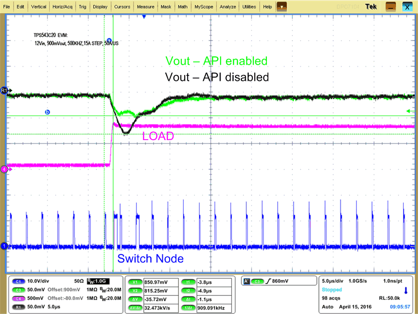
TPS543B20 is a true fixed frequency converter. The major limitation for any fixed frequency converter is that during transient load step up, the converter needs to wait for the next clock cycle to response to the load change, depending on loop bandwidth design and the timing of load transient, this delay time could cause additional output voltage drop. TPS543B20 implements a special circuitry to improve transient performance. During load step up, the converter senses both the speed and the amplitude of the output voltage change, if the output voltage change is fast and big enough, the converter will issue an additional PWM pulse before the next available clock cycle to stop output voltage from further dropping, thus reducing the undershoot voltage.
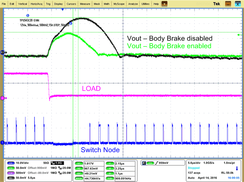
During load step down, TPS543B20 implements a body brake function, that turns off both high-side and lowside FET, and allows power to dissipate through the low-side body diode, reducing overshoot. This approach is very effective while having some impact on efficiency during transient. See Figure 19 and Figure 20.
 Figure 19. Undershoot Comparison with API ON/OFF
  Figure 20. Overshoot Comparison with API ON/OFF