JAJSBF8B June 2011 – April 2018 TPS54478
PRODUCTION DATA.
- 1 特長
- 2 アプリケーション
- 3 概要
- 4 改訂履歴
- 5 Pin Configuration and Functions
- 6 Specifications
-
7 Detailed Description
- 7.1 Overview
- 7.2 Functional Block Diagram
- 7.3
Feature Description
- 7.3.1 Fixed Frequency PWM Control
- 7.3.2 Slope Compensation and Output Current
- 7.3.3 Bootstrap Voltage (BOOT) and Low Dropout Operation
- 7.3.4 Error Amplifier
- 7.3.5 Voltage Reference
- 7.3.6 Adjusting the Output Voltage
- 7.3.7 Enable and Adjusting Undervoltage Lockout
- 7.3.8 Slow Start / Tracking Pin
- 7.3.9 Constant Switching Frequency and Timing Resistor (RT/CLK Pin)
- 7.3.10 Overcurrent Protection
- 7.3.11 START-UP into Prebiased Output
- 7.3.12 Synchronize Using the RT/CLK Pin
- 7.3.13 Power Good (PWRGD Pin)
- 7.3.14 Overvoltage Transient Protection
- 7.3.15 Thermal Shutdown
- 7.3.16 Small Signal Model for Loop Response
- 7.3.17 Simple Small Signal Model for Peak Current Mode Control
- 7.3.18 Small Signal Model for Frequency Compensation
- 7.4 Device Functional Modes
- 7.5 Programming
- 8 Application and Implementation
- 9 Power Supply Recommendations
- 10Layout
- 11デバイスおよびドキュメントのサポート
- 12メカニカル、パッケージ、および注文情報
パッケージ・オプション
メカニカル・データ(パッケージ|ピン)
- RTE|16
サーマルパッド・メカニカル・データ
- RTE|16
発注情報
7.3.8 Slow Start / Tracking Pin
The TPS54478 regulates to the lower of the SS/TR pin and the internal reference voltage. A capacitor on the SS/TR pin to ground implements a slow start time. Before the SS pin reaches the voltage threshold VSSTHR, the charge current is about 45 μA. The TPS54478 internal pull-up current source of 2.2 μA charges the external slow start capacitor after the SS pin voltage exceeds VSSTHR. Equation 4 calculates the required slow start capacitor value where Tss is the desired slow start time in ms and Css is the required capacitance in nF.
vertical spacer

If during normal operation, the VIN goes below the UVLO, EN pin pulled below 1.21 V, or a thermal shutdown event occurs, the TPS54478 stops switching. When the VIN goes above UVLO, EN is released or pulled high, or a thermal shutdown is exited, then SS/TR is discharged to below 65 mV before reinitiating a powering up sequence. The VSENSE voltage will follow the SS/TR pin voltage with a 65mV offset up to 90% of the internal voltage reference. When the SS/TR voltage is greater than 90% of the internal reference voltage the offset increases as the effective system reference transitions from the SS/TR voltage to the internal voltage reference.
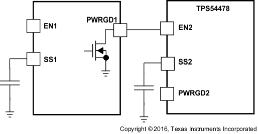 Figure 23. Sequential Start-Up Sequence
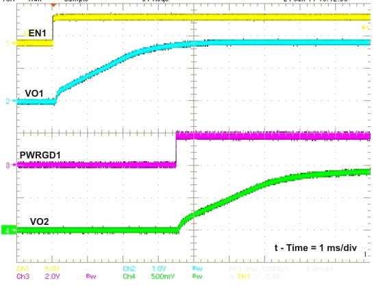 Figure 24. Sequential Startup using EN and PWRGD
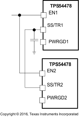 Figure 25. Schematic for Ratio-metric Start-Up Sequence
vertical spacer
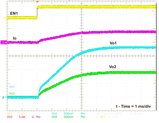 Figure 26. Ratio-metric Startup
Simultaneous power supply sequencing can be implemented by connecting the resistor network of R1 and R2 shown in Figure 27 to the output of the power supply that needs to be tracked or another voltage reference source. Using Equation 5 and Equation 6, the tracking resistors can be calculated. To minimize the effect of the inherent SS/TR to VSENSE offset (Vssoffset) in the slow start circuit and the offset created by the pullup current source (Iss) and tracking resistors, the Vssoffset and Iss are included as variables in the equations. As the SS/TR voltage becomes more than 85% of the nominal reference voltage the Vssoffset becomes larger as the slow start circuits gradually handoff the regulation reference to the internal voltage reference. The SS/TR pin voltage needs to be greater than 0.86 V for a complete handoff to the internal voltage reference as shown in Figure 28.
vertical spacer

vertical spacer

vertical spacer
vertical spacer
vertical spacer
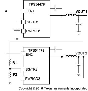 Figure 27. Simultaneous Startup Sequence
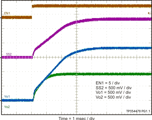 Figure 28. Simultaneous Start-Up using Coupled SS/TR Pins