JAJSBF8B June 2011 – April 2018 TPS54478
PRODUCTION DATA.
- 1 特長
- 2 アプリケーション
- 3 概要
- 4 改訂履歴
- 5 Pin Configuration and Functions
- 6 Specifications
-
7 Detailed Description
- 7.1 Overview
- 7.2 Functional Block Diagram
- 7.3
Feature Description
- 7.3.1 Fixed Frequency PWM Control
- 7.3.2 Slope Compensation and Output Current
- 7.3.3 Bootstrap Voltage (BOOT) and Low Dropout Operation
- 7.3.4 Error Amplifier
- 7.3.5 Voltage Reference
- 7.3.6 Adjusting the Output Voltage
- 7.3.7 Enable and Adjusting Undervoltage Lockout
- 7.3.8 Slow Start / Tracking Pin
- 7.3.9 Constant Switching Frequency and Timing Resistor (RT/CLK Pin)
- 7.3.10 Overcurrent Protection
- 7.3.11 START-UP into Prebiased Output
- 7.3.12 Synchronize Using the RT/CLK Pin
- 7.3.13 Power Good (PWRGD Pin)
- 7.3.14 Overvoltage Transient Protection
- 7.3.15 Thermal Shutdown
- 7.3.16 Small Signal Model for Loop Response
- 7.3.17 Simple Small Signal Model for Peak Current Mode Control
- 7.3.18 Small Signal Model for Frequency Compensation
- 7.4 Device Functional Modes
- 7.5 Programming
- 8 Application and Implementation
- 9 Power Supply Recommendations
- 10Layout
- 11デバイスおよびドキュメントのサポート
- 12メカニカル、パッケージ、および注文情報
パッケージ・オプション
メカニカル・データ(パッケージ|ピン)
- RTE|16
サーマルパッド・メカニカル・データ
- RTE|16
発注情報
7.3.18 Small Signal Model for Frequency Compensation
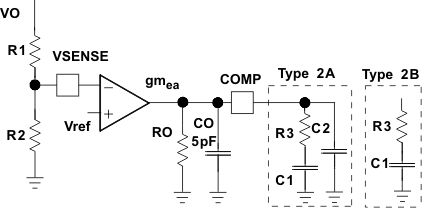
The TPS54478 uses a transconductance amplifier for the error amplifier and readily supports two of the commonly used frequency compensation circuits. The compensation circuits are shown in Figure 33. The Type 2 circuits are most likely implemented in high bandwidth power supply designs using low ESR output capacitors. In Type 2A, one additional high frequency pole is added to attenuate high frequency noise.
 Figure 33. Type-II of Frequency Compensation
The design guidelines for TPS54478 loop compensation are addressed in the Application Information section with more details. The approach is to run the Pspice model first to find the accurate response of the power stage with slope compensation effect. The compensation network is then designed based on the desired crossover frequency. The crossover frequency and phase margin are more closer to the measured results when the slope compensation effect is included.
For type-II compensation, the modulator pole, fpmod, and the esr zero, fz1 can be calculated using Equation 13 and Equation 14. Derating the output capacitor (COUT) is needed if the output voltage is a high percentage of the capacitor rating. Use the capacitor manufacturer information to derate the capacitor value. Use Equation 15 and Equation 16 to estimate a starting point for the crossover frequency, fc. Equation 15 is the geometric mean of the modulator pole and the esr zero and Equation 16 is the mean of modulator pole and the switching frequency. Use the lower value of Equation 15 or Equation 16 as the maximum crossover frequency.

vertical spacer

vertical spacer

vertical spacer

vertical spacer
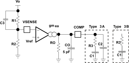
The type-III compensation is recommended to achieve higher crossover frequency by introducing extra phase lift. By adding a small capacitor C3 in parallel with R1, one-pair of zero and pole is generated as given by Equation 17 and Equation 18. The Application Information section provides step-by-step design guidelines for Type-III compensation with the effect of slope compensation included.
 Figure 34. Type-III of Frequency Compensation

