JAJSBU6B May 2013 – October 2023 TPS54531
PRODUCTION DATA
- 1
- 1 特長
- 2 アプリケーション
- 3 概要
- 4 Revision History
- 5 Pin Configuration and Functions
- 6 Specifications
-
7 Detailed Description
- 7.1 Overview
- 7.2 Functional Block Diagram
- 7.3
Feature Description
- 7.3.1 Fixed-Frequency PWM Control
- 7.3.2 Voltage Reference (Vref)
- 7.3.3 Bootstrap Voltage (BOOT)
- 7.3.4 Enable and Adjustable Input Undervoltage Lockout (VIN UVLO)
- 7.3.5 Programmable Slow Start Using SS Pin
- 7.3.6 Error Amplifier
- 7.3.7 Slope Compensation
- 7.3.8 Current-Mode Compensation Design
- 7.3.9 Overcurrent Protection and Frequency Shift
- 7.3.10 Overvoltage Transient Protection
- 7.3.11 Thermal Shutdown
- 7.4 Device Functional Modes
-
8 Application and Implementation
- 8.1 Application Information
- 8.2
Typical Application
- 8.2.1 Design Requirements
- 8.2.2
Detailed Design Procedure
- 8.2.2.1 Custom Design With WEBENCH® Tools
- 8.2.2.2 Switching Frequency
- 8.2.2.3 Output Voltage Set Point
- 8.2.2.4 Undervoltage Lockout Set Point
- 8.2.2.5 Input Capacitors
- 8.2.2.6 Output Filter Components
- 8.2.2.7 Compensation Components
- 8.2.2.8 Bootstrap Capacitor
- 8.2.2.9 Catch Diode
- 8.2.2.10 Slow-Start Capacitor
- 8.2.2.11 Output Voltage Limitations
- 8.2.2.12 Power Dissipation Estimate
- 8.2.3 Application Curves
- 8.3 Power Supply Recommendations
- 8.4 Layout
- 9 Device and Documentation Support
- 10Mechanical, Packaging, and Orderable Information
パッケージ・オプション
メカニカル・データ(パッケージ|ピン)
- DDA|8
サーマルパッド・メカニカル・データ
- DDA|8
発注情報
8.2.3 Application Curves
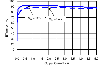 Figure 8-3 Efficiency
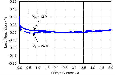 Figure 8-5 Load
Regulation
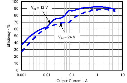 Figure 8-4 Low-Current Efficiency
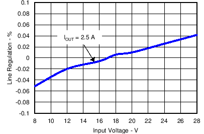 Figure 8-6 Line
Regulation
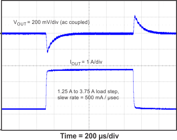 Figure 8-7 Transient Response
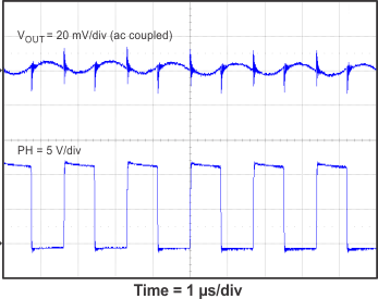 Figure 8-9 Full-Load Output Ripple
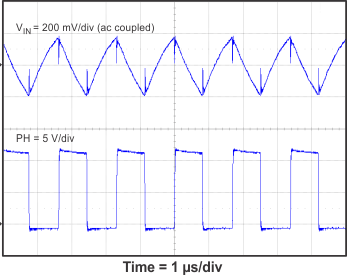 Figure 8-11 Full-Load Input Ripple
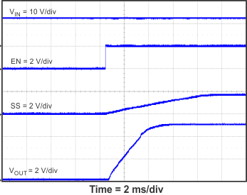 Figure 8-13 Startup Relative to Enable
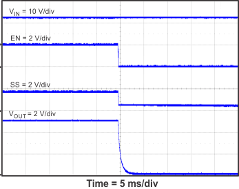 Figure 8-15 Shut
Down Relative to EN
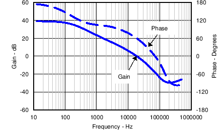 Figure 8-8 Loop
Response
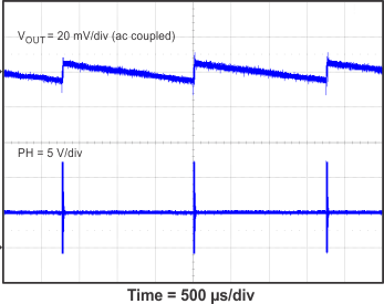 Figure 8-10 Eco-mode Output Ripple
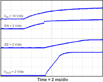 Figure 8-12 Startup Relative to VIN
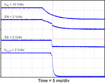 Figure 8-14 Shut
Down Relative to VIN