JAJSBO6B June 2012 – May 2019 TPS54678
PRODUCTION DATA.
- 1 特長
- 2 アプリケーション
- 3 概要
- 4 改訂履歴
- 5 概要(続き)
- 6 Pin Configuration and Functions
- 7 Specifications
-
8 Detailed Description
- 8.1 Overview
- 8.2 Functional Block Diagram
- 8.3
Feature Description
- 8.3.1 Fixed Frequency PWM Control
- 8.3.2 Slope Compensation and Output Current
- 8.3.3 Bootstrap Voltage (Boot) and Low Dropout Operation
- 8.3.4 Error Amplifier
- 8.3.5 Voltage Reference
- 8.3.6 Adjusting the Output Voltage
- 8.3.7 Enable and Adjusting Undervoltage Lockout
- 8.3.8 Soft-Start Pin
- 8.3.9 Sequencing
- 8.3.10 Constant Switching Frequency and Timing Resistor (RT/CLK Pin)
- 8.3.11 Overcurrent Protection
- 8.3.12 Safe Start-Up into Prebiased Outputs
- 8.3.13 Synchronize Using the RT/CLK Pin
- 8.3.14 Power Good (PWRGD Pin)
- 8.3.15 Overvoltage Transient Protection
- 8.3.16 Thermal Shutdown
- 8.4 Device Functional Modes
-
9 Application and Implementation
- 9.1 Application Information
- 9.2
Typical Application
- 9.2.1 Design Requirements
- 9.2.2
Detailed Design Procedure
- 9.2.2.1 Custom Design With WEBENCH® Tools
- 9.2.2.2 Step One: Select the Switching Frequency
- 9.2.2.3 Step Two: Select the Output Inductor
- 9.2.2.4 Step Three: Choose the Output Capacitor
- 9.2.2.5 Step Four: Select the Input Capacitor
- 9.2.2.6 Step Five: Choose the Soft-Start Capacitor
- 9.2.2.7 Step Six: Select the Bootstrap Capacitor
- 9.2.2.8 Step Eight: Select Output Voltage and Feedback Resistors
- 9.2.2.9 Step Nine: Select Loop Compensation Components
- 9.2.3 Application Curves
- 10Power Supply Recommendations
- 11Layout
- 12デバイスおよびドキュメントのサポート
- 13メカニカル、パッケージ、および注文情報
パッケージ・オプション
メカニカル・データ(パッケージ|ピン)
- RTE|16
サーマルパッド・メカニカル・データ
- RTE|16
発注情報
8.3.10 Constant Switching Frequency and Timing Resistor (RT/CLK Pin)
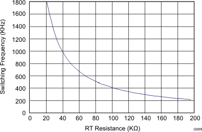
The switching frequency of the TPS54678 is adjustable over a wide range from approximately 200 kHz to
2000 kHz by placing a maximum of 210 kΩ and minimum of 18 kΩ, respectively, on the RT/CLK pin. The RT/CLK is typically 0.5 V. To determine the timing resistance for a given switching frequency, use the curve in Figure 24. To reduce the solution size one would typically set the switching frequency as high as possible, but tradeoffs of the supply efficiency, maximum input voltage and minimum controllable on time should be considered.
The minimum controllable on time is typically 85 ns at 3-A current load and 100 ns at no load, and will limit the maximum operating input voltage or output voltage.

 Figure 24. Switching Frequency vs RT Set Resistor