JAJSBO6B June   2012  – May 2019 TPS54678

PRODUCTION DATA.  

  1. 特長
  2. アプリケーション
  3. 概要
    1.     Device Images
      1.      概略回路図
      2.      効率と出力電流との関係
  4. 改訂履歴
  5. 概要(続き)
  6. Pin Configuration and Functions
    1.     Pin Functions
  7. Specifications
    1. 7.1 Absolute Maximum Ratings
    2. 7.2 ESD Ratings
    3. 7.3 Recommended Operating Conditions
    4. 7.4 Thermal Information
    5. 7.5 Electrical Characteristics
    6. 7.6 Typical Characteristics
  8. Detailed Description
    1. 8.1 Overview
    2. 8.2 Functional Block Diagram
    3. 8.3 Feature Description
      1. 8.3.1  Fixed Frequency PWM Control
      2. 8.3.2  Slope Compensation and Output Current
      3. 8.3.3  Bootstrap Voltage (Boot) and Low Dropout Operation
      4. 8.3.4  Error Amplifier
      5. 8.3.5  Voltage Reference
      6. 8.3.6  Adjusting the Output Voltage
      7. 8.3.7  Enable and Adjusting Undervoltage Lockout
      8. 8.3.8  Soft-Start Pin
      9. 8.3.9  Sequencing
      10. 8.3.10 Constant Switching Frequency and Timing Resistor (RT/CLK Pin)
      11. 8.3.11 Overcurrent Protection
        1. 8.3.11.1 High-Side Overcurrent Protection
        2. 8.3.11.2 Low-Side Overcurrent Protection
      12. 8.3.12 Safe Start-Up into Prebiased Outputs
      13. 8.3.13 Synchronize Using the RT/CLK Pin
      14. 8.3.14 Power Good (PWRGD Pin)
      15. 8.3.15 Overvoltage Transient Protection
      16. 8.3.16 Thermal Shutdown
    4. 8.4 Device Functional Modes
      1. 8.4.1 Small Signal Model for Loop Response
      2. 8.4.2 Simple Small Signal Model for Peak Current Mode Control
      3. 8.4.3 Small Signal Model for Frequency Compensation
  9. Application and Implementation
    1. 9.1 Application Information
    2. 9.2 Typical Application
      1. 9.2.1 Design Requirements
      2. 9.2.2 Detailed Design Procedure
        1. 9.2.2.1 Custom Design With WEBENCH® Tools
        2. 9.2.2.2 Step One: Select the Switching Frequency
        3. 9.2.2.3 Step Two: Select the Output Inductor
        4. 9.2.2.4 Step Three: Choose the Output Capacitor
        5. 9.2.2.5 Step Four: Select the Input Capacitor
        6. 9.2.2.6 Step Five: Choose the Soft-Start Capacitor
        7. 9.2.2.7 Step Six: Select the Bootstrap Capacitor
        8. 9.2.2.8 Step Eight: Select Output Voltage and Feedback Resistors
          1. 9.2.2.8.1 Output Voltage Limitations
        9. 9.2.2.9 Step Nine: Select Loop Compensation Components
      3. 9.2.3 Application Curves
        1. 9.2.3.1 Additional Information About Application Curves
          1. 9.2.3.1.1 Efficiency
          2. 9.2.3.1.2 Voltage Ripple Measurements
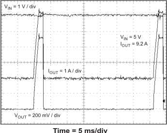
          3. 9.2.3.1.3 Start-Up and Shutdown Waveforms
          4. 9.2.3.1.4 Hiccup Mode Current Limit
  10. 10Power Supply Recommendations
  11. 11Layout
    1. 11.1 Layout Guidelines
    2. 11.2 Layout Example
    3. 11.3 Power Dissipation Estimate
  12. 12デバイスおよびドキュメントのサポート
    1. 12.1 デバイス・サポート
      1. 12.1.1 デベロッパー・ネットワークの製品に関する免責事項
      2. 12.1.2 開発サポート
        1. 12.1.2.1 WEBENCH®ツールによるカスタム設計
    2. 12.2 ドキュメントのサポート
      1. 12.2.1 関連資料
    3. 12.3 ドキュメントの更新通知を受け取る方法
    4. 12.4 コミュニティ・リソース
    5. 12.5 商標
    6. 12.6 静電気放電に関する注意事項
    7. 12.7 Glossary
  13. 13メカニカル、パッケージ、および注文情報

パッケージ・オプション

メカニカル・データ(パッケージ|ピン)
サーマルパッド・メカニカル・データ
発注情報

Hiccup Mode Current Limit

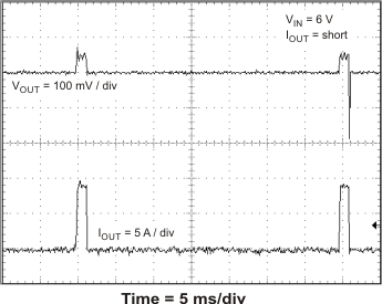
The TPS54678 has hiccup mode current limit. When the peak switch current exceeds the current limit threshold, the device shuts down and restarts. Hiccup mode current limit operation is shown in Figure 46 and Figure 47. Figure 46 shows the hiccup mode current limit with a slight resistive overload. When the peak current limit is exceeded, the output voltage is disabled. Figure 47 shows the operation of the TPS54678 with the output shorted to ground. The device continuously resets until the fault condition is removed.
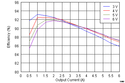
TPS54678 ai_g002_lvsbf3.png
Figure 32. Efficiency vs Load Current
TPS54678 ai_g003_lvsbf3.png
Figure 33. Load Regulation
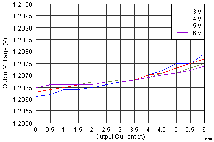
TPS54678 ai_g004_lvsbf3.png
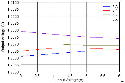
Figure 34. Line Regulation
TPS54678 ai_g005_lvsbf3.png
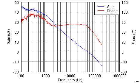
Figure 36. Loop Response
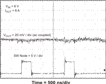
TPS54678 ai_output_ripple_6V6A_lvsbf3.gif
VIN = 6 V, IOUT = 6 A
Figure 38. Output Ripple
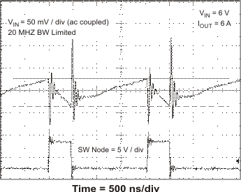
TPS54678 ai_input_ripple_6V6A_lvsbf3.gif
VIN = 6 V, IOUT = 6 A
Figure 40. Input Ripple
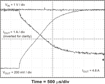
TPS54678 ai_startup_enable_lvsbf3.gif
Figure 42. Start-Up Relative to Enable
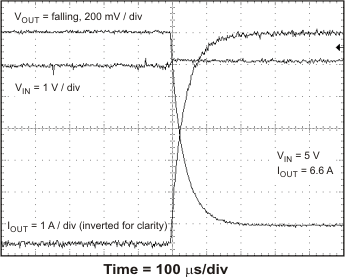
TPS54678 ai_shutdown_Vin_lvsbf3.gif
Figure 44. Shutdown Relative to VIN
TPS54678 ai_Hiccup_shutdown_lvsbf3.gif
Figure 46. Hiccup Mode Current Limit Shutdown
TPS54678 ai_transient_plot_lvsbf3.gif
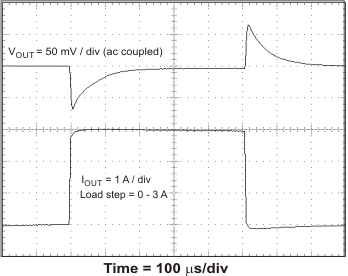
Figure 35. Transient Response
TPS54678 ai_output_ripple_plot_lvsbf3.gif
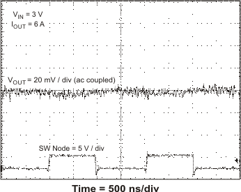
VIN = 3 V, IOUT = 6 A
Figure 37. Output Ripple
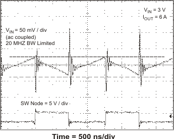
TPS54678 ai_input_ripple_3V6A_lvsbf3.gif
VIN = 3 V, IOUT = 6 A
Figure 39. Input Ripple
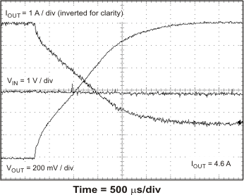
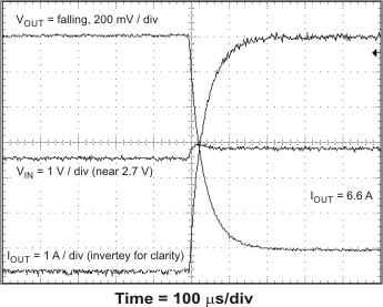
TPS54678 ai_startup_Vin_lvsbf3.gif
Figure 41. Start-Up Relative to VIN
TPS54678 ai_startup_enable_lvsbf3.gif
Figure 43. Start-Up into Prebias
TPS54678 ai_shutdown_EN_lvsbf3.gif
Figure 45. Shutdown Relative to Enable
TPS54678 ai_Hiccup_restart_lvsbf3.gif
Figure 47. Hiccup Mode Current Limit Restart into Short Circuit