JAJSQ82B November 2023 – July 2024 TPS548D26
PRODUCTION DATA
- 1
- 1 特長
- 2 アプリケーション
- 3 概要
- 4 Pin Configuration and Functions
- 5 Specifications
-
6 Detailed Description
- 6.1 Overview
- 6.2 Functional Block Diagram
- 6.3
Feature Description
- 6.3.1 Internal VCC LDO and Using an External Bias on the VCC and VDRV Pin
- 6.3.2 Input Undervoltage Lockout (UVLO)
- 6.3.3 Set the Output Voltage
- 6.3.4 Differential Remote Sense and Feedback Divider
- 6.3.5 Start-Up and Shutdown
- 6.3.6 Loop Compensation
- 6.3.7 Set Switching Frequency and Operation Mode
- 6.3.8 Switching Node (SW)
- 6.3.9 Overcurrent Limit and Low-side Current Sense
- 6.3.10 Negative Overcurrent Limit
- 6.3.11 Zero-Crossing Detection
- 6.3.12 Input Overvoltage Protection
- 6.3.13 Output Undervoltage and Overvoltage Protection
- 6.3.14 Overtemperature Protection
- 6.3.15 Power Good
- 6.4 Device Functional Modes
- 7 Application and Implementation
- 8 Device and Documentation Support
- 9 Revision History
- 10Mechanical, Packaging, and Orderable Information
6.4.2 Auto-Skip Eco-mode Light Load Operation
When the operation mode is set to DCM, the device automatically reduces the switching frequency at light-load conditions to maintain high efficiency. This section describes the operation in detail.
As the output current decreases from heavy load condition, the inductor current also decreases until the rippled valley of the inductor current touches zero level. Zero level is the boundary between the continuous-conduction and discontinuous-conduction modes. The synchronous MOSFET turns off when this zero inductor current is detected. As the load current decreases further, the converter runs into discontinuous-conduction mode (DCM). The on-time is maintained to a level approximately the same as during continuous-conduction mode operation so that discharging the output capacitor with a smaller load current to the level of the reference voltage requires more time. Calculate the transition point to the light-load operation IOUT(LL) (for example, the threshold between continuous- and discontinuous-conduction mode) using the following equation.
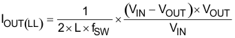
where
- fSW is the switching frequency
TI recommends using low ESR capacitors (such as ceramic capacitor) for skip-mode.