JAJSDE0A June 2017 – February 2024 TPS549B22
PRODUCTION DATA
- 1
- 1 特長
- 2 アプリケーション
- 3 概要
- 4 Pin Configuration and Functions
- 5 Specifications
-
6 Detailed Description
- 6.1 Overview
- 6.2 Functional Block Diagram
- 6.3 Feature Description
- 6.4 Device Functional Modes
- 6.5 Programming
-
7 Register Maps
- 7.1 OPERATION Register (address = 1h)
- 7.2 ON_OFF_CONFIG Register (address = 2h)
- 7.3 CLEAR FAULTS (address = 3h)
- 7.4 WRITE PROTECT (address = 10h)
- 7.5 STORE_DEFAULT_ALL (address = 11h)
- 7.6 RESTORE_DEFAULT_ALL (address = 12h)
- 7.7 CAPABILITY (address = 19h)
- 7.8 VOUT_MODE (address = 20h)
- 7.9 VOUT_COMMAND (address = 21h)
- 7.10 VOUT_MARGIN_HIGH (address = 25h) ®
- 7.11 VOUT_MARGIN_LOW (address = 26h)
- 7.12 STATUS_BYTE (address = 78h)
- 7.13 STATUS_WORD (High Byte) (address = 79h)
- 7.14 STATUS_VOUT (address = 7Ah)
- 7.15 STATUS_IOUT (address = 7Bh)
- 7.16 STATUS_CML (address = 7Eh)
- 7.17 MFR_SPECIFIC_00 (address = D0h)
- 7.18 MFR_SPECIFIC_01 (address = D1h)
- 7.19 MFR_SPECIFIC_02 (address = D2h)
- 7.20 MFR_SPECIFIC_03 (address = D3h)
- 7.21 MFR_SPECIFIC_04 (address = D4h)
- 7.22 MFR_SPECIFIC_06 (address = D6h)
- 7.23 MFR_SPECIFIC_07 (address = D7h)
- 7.24 MFR_SPECIFIC_44 (address = FCh)
-
8 Application and Implementation
- 8.1 Application Information
- 8.2
Typical Applications
- 8.2.1 TPS549B22 1.5-V to 18-V Input, 1-V Output, 25-A Converter
- 8.2.2 Design Requirements
- 8.2.3
Detailed Design Procedure
- 8.2.3.1 Custom Design With WEBENCH® Tools
- 8.2.3.2 Switching Frequency Selection
- 8.2.3.3 Inductor Selection
- 8.2.3.4 Output Capacitor Selection
- 8.2.3.5 Input Capacitor Selection
- 8.2.3.6 Bootstrap Capacitor Selection
- 8.2.3.7 BP Pin
- 8.2.3.8 R-C Snubber and VIN Pin High-Frequency Bypass
- 8.2.3.9 Optimize Reference Voltage (VSEL)
- 8.2.3.10 MODE Pin Selection
- 8.2.3.11 ADDR Pin Selection
- 8.2.3.12 Overcurrent Limit Design
- 8.2.4 Application Curves
- 8.3 Power Supply Recommendations
- 8.4 Layout
- 9 Device and Documentation Support
- 10Revision History
- 11Mechanical, Packaging, and Orderable Information
パッケージ・オプション
デバイスごとのパッケージ図は、PDF版データシートをご参照ください。
メカニカル・データ(パッケージ|ピン)
- RVF|40
サーマルパッド・メカニカル・データ
- RVF|40
発注情報
8.2.3.4.3 Output Voltage Ripple
The output voltage ripple is another important design consideration. Equation 10 calculates the minimum output capacitance required to meet the output voltage ripple specification. This criterion is the requirement when the impedance of the output capacitance is dominated by ESR.
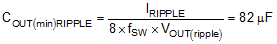
In this case, the maximum output voltage ripple is 10 mV. For this requirement, the minimum capacitance for ripple requirement yields 82 µF. Because this capacitance value is significantly lower compared to that of transient requirement, determine the capacitance bank from steps in the previous section Section 8.2.3.4.2. Because the output capacitor bank consists of both POSCAP and MLCC type capacitors, it is important to consider the ripple effect at the switching frequency due to effective ESR. Use Equation 11 to determine the maximum ESR of the output capacitor bank for the switching frequency.
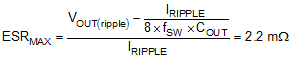
Estimate the effective ESR at the switching frequency by obtaining the impedance vs frequency characteristics of the output capacitors. The parallel impedance of capacitor bank 1 and capacitor bank 2 at the switching frequency of the design example is estimated to be 1.2 mΩ, which is less than that of the maximum ESR value. Therefore, the output voltage ripple requirement (10 mV) can be met. For detailed calculation on the effective ESR please contact the factory to obtain a user-friendly Excel based design tool.