JAJSIP2B November 2018 – December 2020 TPS55288
PRODUCTION DATA
- 1 特長
- 2 アプリケーション
- 3 概要
- 4 Revision History
- 5 Pin Configuration and Functions
- 6 Specifications
-
7 Detailed Description
- 7.1 Overview
- 7.2 Functional Block Diagram
- 7.3
Feature Description
- 7.3.1 VCC Power Supply
- 7.3.2 Operation Mode Setting
- 7.3.3 Input Undervoltage Lockout
- 7.3.4 Enable and Programmable UVLO
- 7.3.5 Soft Start
- 7.3.6 Shutdown and Load Discharge
- 7.3.7 Switching Frequency
- 7.3.8 Switching Frequency Dithering
- 7.3.9 Inductor Current Limit
- 7.3.10 Internal Charge Path
- 7.3.11 Output Voltage Setting
- 7.3.12 Output Current Monitoring and Cable Voltage Droop Compensation
- 7.3.13 Integrated Gate Drivers
- 7.3.14 Output Current Limit
- 7.3.15 Overvoltage Protection
- 7.3.16 Output Short Circuit Protection
- 7.3.17 Thermal Shutdown
- 7.4 Device Functional Modes
- 7.5 I2C Serial Interface
- 7.6
Register Maps
- 7.6.1 REF Register (Address = 0h, 1h) [reset = 11010010h, 00000000h]
- 7.6.2 IOUT_LIMIT Register (Address = 2h) [reset = 11100100h]
- 7.6.3 VOUT_SR Register (Address = 3h) [reset = 00000001h]
- 7.6.4 VOUT_FS Register (Address = 4h) [reset = 00000011h]
- 7.6.5 CDC Register (Address = 5h) [reset = 11100000h]
- 7.6.6 MODE Register (Address = 6h) [reset = 00100000h]
- 7.6.7 STATUS Register (Address = 7h) [reset = 00000011h]
- 7.6.8 Register Summary
- 8 Application and Implementation
- 9 Power Supply Recommendations
- 10Layout
- 11Device and Documentation Support
- 12Mechanical, Packaging, and Orderable Information
パッケージ・オプション
メカニカル・データ(パッケージ|ピン)
- RPM|26
サーマルパッド・メカニカル・データ
- RPM|26
発注情報
7.5.1 Data Validity
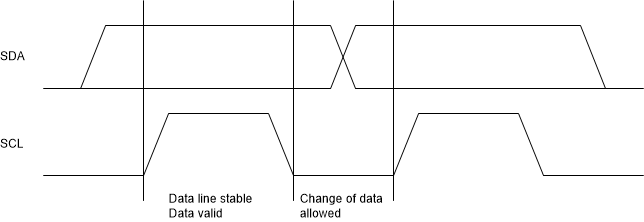
The data on the SDA line must be stable during the high level period of the clock. The high level or low level state of the data line can only change when the clock signal on the SCL line is low level. One clock pulse is generated for each data bit transferred.
 Figure 7-7 I2C Data Validity