JAJSO91 December 2023 TPS55289-Q1
PRODUCTION DATA
- 1
- 1 特長
- 2 アプリケーション
- 3 概要
- 4 Pin Configuration and Functions
- 5 Specifications
-
6 Detailed Description
- 6.1 Overview
- 6.2 Functional Block Diagram
- 6.3
Feature Description
- 6.3.1 VCC Power Supply
- 6.3.2 EXTVCC Power Supply
- 6.3.3 I2C Address Selection
- 6.3.4 Input Undervoltage Lockout
- 6.3.5 Enable and Programmable UVLO
- 6.3.6 Soft Start
- 6.3.7 Shutdown and Load Discharge
- 6.3.8 Switching Frequency
- 6.3.9 Switching Frequency Dithering
- 6.3.10 Inductor Current Limit
- 6.3.11 Internal Charge Path
- 6.3.12 Output Voltage Setting
- 6.3.13 Output Current Monitoring and Cable Voltage Droop Compensation
- 6.3.14 Output Current Limit
- 6.3.15 Overvoltage Protection
- 6.3.16 Output Short Circuit Protection
- 6.3.17 Thermal Shutdown
- 6.4 Device Functional Modes
- 6.5 Programming
-
7 Register Maps
- 7.1 REF Register (Address = 0h, 1h) [reset = 10100100b, 00000001b]
- 7.2 IOUT_LIMIT Register (Address = 2h) [reset = 11100100b]
- 7.3 VOUT_SR Register (Address = 3h) [reset = 00000001b]
- 7.4 VOUT_FS Register (Address = 4h) [reset = 00000011b]
- 7.5 CDC Register (Address = 5h) [reset = 11100000b]
- 7.6 MODE Register (Address = 6h) [reset = 00100000b]
- 7.7 STATUS Register (Address = 7h) [reset = 00000011b]
- 7.8 Register Summary
- 8 Application and Implementation
- 9 Device and Documentation Support
- 10Revision History
- 11Mechanical, Packaging, and Orderable Information
6.3.12 Output Voltage Setting
There are two ways to set the output voltage: changing the feedback ratio and changing the reference voltage. The TPS55289-Q1 has a 11-bit DAC to program the reference voltage from 45mV to 1.2V. The TPS55289-Q1 also can select an internal feedback resistor divider or an external resistor divider by setting the FB bit in register 04h. When the FB bit is set to 0, the output voltage feedback ratio is set in internal register 04h. When the FB bit is set to 1, the output voltage feedback ratio is set by an external resistor divider.
When using internal output voltage feedback settings, there are four feedback ratios programmable by writing the INTFB[1:0] bits of register 04h. With this function, the TPS55289-Q1 can limit the maximum output voltage to different values. In addition, the minimum step of the output voltage change is also programmed to 10mV, 7.5mV, 5mV, and 2.5mV, accordingly.
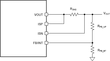
When using an external output voltage feedback resistor divider as shown in Figure 6-5, use Equation 5 to calculate the output voltage with the reference voltage at the FB/INT pin.

 Figure 6-5 Output Voltage
Setting by External Resistor Divider
Figure 6-5 Output Voltage
Setting by External Resistor DividerTI recommends using 100kΩ for the up resistor RFB_UP. The reference voltage VREF at the FB/INT pin is programmable from 45mV to 1.2V by writing a 11-bit data into register 00h and 01h.