JAJSGT7B May 2013 – January 2019 TPS55330
PRODUCTION DATA.
- 1 特長
- 2 アプリケーション
- 3 概要
- 4 改訂履歴
- 5 Pin Configuration and Functions
- 6 Specifications
- 7 Detailed Description
-
8 Application and Implementation
- 8.1 Application Information
- 8.2
Typical Application
- 8.2.1 Design Requirements
- 8.2.2
Detailed Design Procedure
- 8.2.2.1 Custom Design With WEBENCH® Tools
- 8.2.2.2 Selecting the Switching Frequency (R4)
- 8.2.2.3 Determining the Duty Cycle
- 8.2.2.4 Selecting the Inductor (L1)
- 8.2.2.5 Computing the Maximum Output Current
- 8.2.2.6 Selecting the Output Capacitor (C8-C10)
- 8.2.2.7 Selecting the Input Capacitors (C2, C7)
- 8.2.2.8 Setting Output Voltage (R1, R2)
- 8.2.2.9 Setting the Soft-start Time (C7)
- 8.2.2.10 Selecting the Schottky Diode (D1)
- 8.2.2.11 Compensating the Control Loop (R3, C4, C5)
- 8.2.3 Application Curves
- 9 Power Supply Recommendations
- 10Layout
- 11デバイスおよびドキュメントのサポート
- 12メカニカル、パッケージ、および注文情報
パッケージ・オプション
メカニカル・データ(パッケージ|ピン)
- RTE|16
サーマルパッド・メカニカル・データ
- RTE|16
発注情報
6.6 Typical Characteristics
VIN = 5 V, TA = 25°C (unless otherwise noted)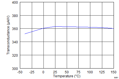 Figure 1. Error Amplifier Transconductance vs Temperature
 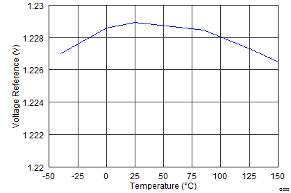 Figure 3. Feedback Voltage Reference vs Temperature
 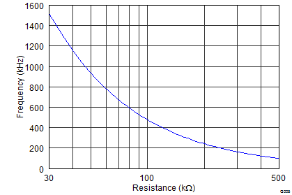 Figure 5. Frequency vs FREQ Resistance
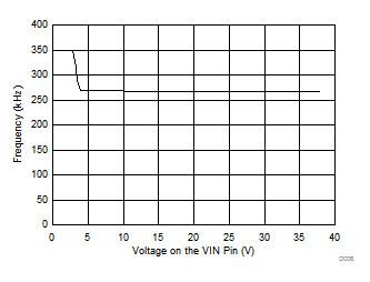
| TA = 25°C |
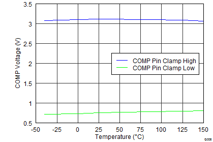 Figure 9. COMP Clamp Voltage vs Temperature
 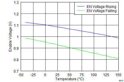 Figure 11. Enable Voltage vs Temperature
 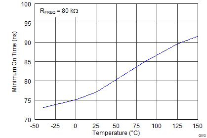 Figure 13. Minimum On Time vs Temperature
 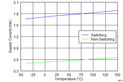 Figure 15. Supply Current vs Temperature
 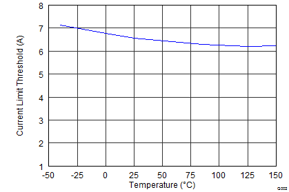 Figure 2. Switch Current Limit vs Temperature
 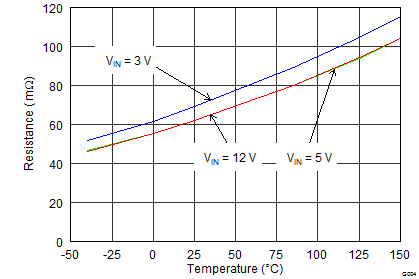 Figure 4. RDS(ON) vs Temperature
 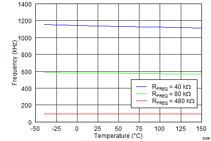 Figure 6. Frequency vs Temperature
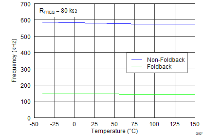
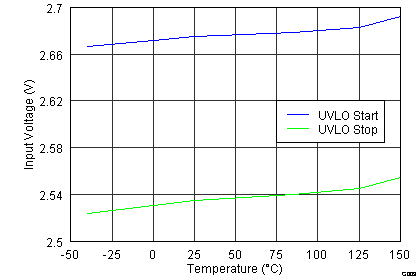 Figure 10. Input Voltage UVLO vs Temperature
 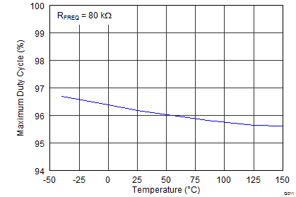 Figure 12. Maximum Duty Cycle vs Temperature
 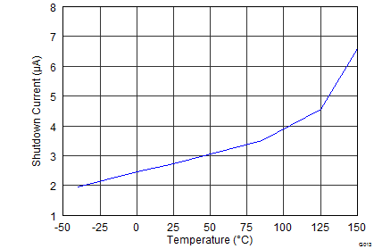 Figure 14. Shutdown Current vs Temperature