JAJSCP3 November   2016 TPS562210A , TPS563210A

PRODUCTION DATA.  

  1. 特長
  2. アプリケーション
  3. 概要
  4. 改訂履歴
  5. Pin Configuration and Functions
  6. Specifications
    1. 6.1 Absolute Maximum Ratings
    2. 6.2 ESD Ratings
    3. 6.3 Recommended Operating Conditions
    4. 6.4 Thermal Information
    5. 6.5 Electrical Characteristics
    6. 6.6 Timing Requirements
    7. 6.7 Typical Characteristics
      1. 6.7.1 TPS562210A Characteristics
      2. 6.7.2 TPS563210A Characteristics
  7. Detailed Description
    1. 7.1 Overview
    2. 7.2 Functional Block Diagram
    3. 7.3 Feature Description
      1. 7.3.1 The Adaptive On-Time Control and PWM Operation
      2. 7.3.2 Soft Start and Pre-Biased Soft Start
      3. 7.3.3 Power Good
      4. 7.3.4 Current Protection
      5. 7.3.5 Over Voltage Protection
      6. 7.3.6 UVLO Protection
      7. 7.3.7 Thermal Shutdown
    4. 7.4 Device Functional Modes
      1. 7.4.1 Advanced Eco-Mode™ Control
  8. Application and Implementation
    1. 8.1 Application Information
    2. 8.2 Typical Application
      1. 8.2.1 Typical Application, TPS562210A
        1. 8.2.1.1 Design Requirements
        2. 8.2.1.2 Detailed Design Procedure
          1. 8.2.1.2.1 Output Voltage Resistors Selection
          2. 8.2.1.2.2 Output Filter Selection
          3. 8.2.1.2.3 Input Capacitor Selection
          4. 8.2.1.2.4 Bootstrap capacitor Selection
        3. 8.2.1.3 Application Curves
      2. 8.2.2 Typical Application, TPS563210A
        1. 8.2.2.1 Design Requirements
        2. 8.2.2.2 Detailed Design Procedures
          1. 8.2.2.2.1 Output Filter Selection
        3. 8.2.2.3 Application Curves
  9. Power Supply Recommendations
  10. 10Layout
    1. 10.1 Layout Guidelines
    2. 10.2 Layout Example
  11. 11デバイスおよびドキュメントのサポート
    1. 11.1 デバイス・サポート
    2. 11.2 関連リンク
    3. 11.3 ドキュメントの更新通知を受け取る方法
    4. 11.4 コミュニティ・リソース
    5. 11.5 商標
    6. 11.6 静電気放電に関する注意事項
    7. 11.7 用語集
  12. 12メカニカル、パッケージ、および注文情報

パッケージ・オプション

メカニカル・データ(パッケージ|ピン)
サーマルパッド・メカニカル・データ
発注情報

Layout

Layout Guidelines

  1. VIN and GND traces should be as wide as possible to reduce trace impedance. The wide areas are also of advantage from the view point of heat dissipation.
  2. The input capacitor and output capacitor should be placed as close to the device as possible to minimize trace impedance.
  3. Provide sufficient vias for the input capacitor and output capacitor.
  4. Keep the SW trace as physically short and wide as practical to minimize radiated emissions.
  5. Do not allow switching current to flow under the device.
  6. A separate VOUT path should be connected to the upper feedback resistor.
  7. Make a Kelvin connection to the GND pin for the feedback path.
  8. Voltage feedback loop should be placed away from the high-voltage switching trace, and preferably has ground shield.
  9. The trace of the VFB node should be as small as possible to avoid noise coupling.
  10. The GND trace between the output capacitor and the GND pin should be as wide as possible to minimize its trace impedance.

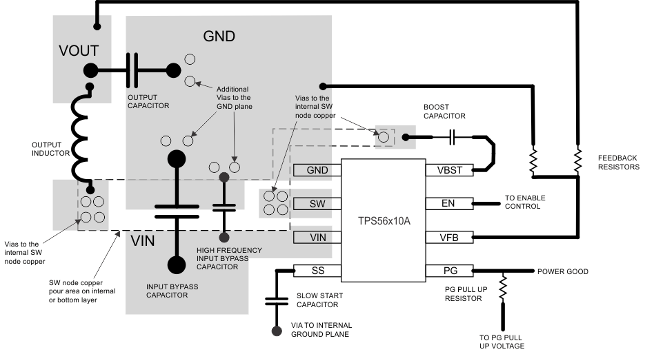
Layout Example

TPS562210A TPS563210A Layout_slvsdp9.gif