JAJSJQ6 September 2020 TPS563207
PRODUCTION DATA
- 1 特長
- 2 アプリケーション
- 3 概要
- 4 Revision History
- 5 Device Comparison Table
- 6 Pin Configuration and Functions
- 7 Specifications
- 8 Detailed Description
- 9 Application and Implementation
- 10Power Supply Recommendations
- 11Layout
- 12Device and Documentation Support
- 13Mechanical, Packaging, and Orderable Information
9.2.3 Application Curves
Below waveforms are tested at VIN = 12 V, unless otherwise noted.
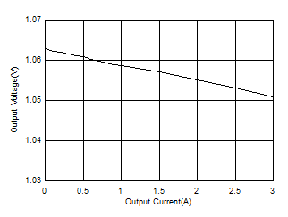 Figure 9-2 Load Regulation with
Different Loading
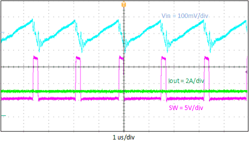 Figure 9-4 Input Voltage Ripple Iout
= 3 A
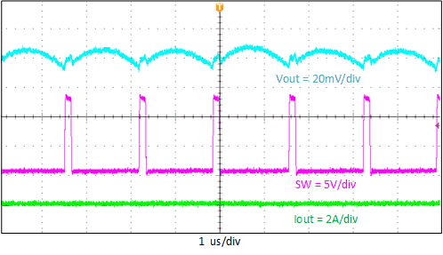 Figure 9-6 Output Voltage Ripple,
Iout = 10 mA
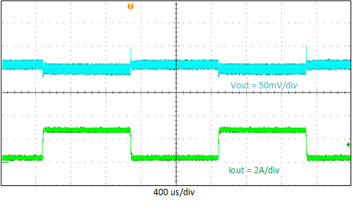 Figure 9-8 Transient Load Response,
Iout = 0.3 to 2.7 A
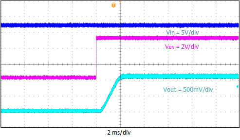 Figure 9-10 Start-Up Relative to
EN
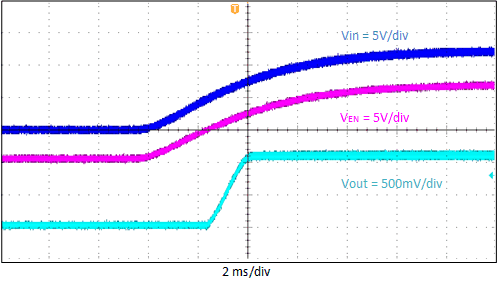 Figure 9-12 Start Up Relative to
VIN
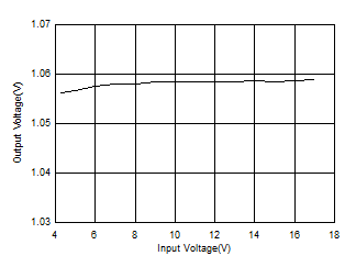 Figure 9-3 Load Regulation with
Different Input Voltage
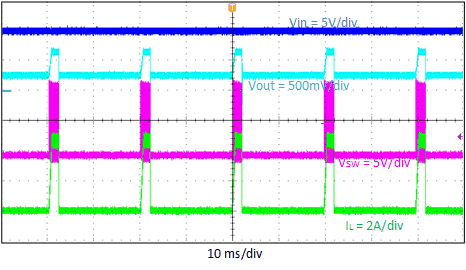 Figure 9-5 Hiccup (Short Vout
Test)
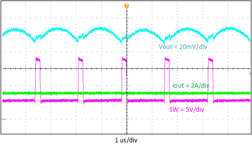 Figure 9-7 Output Voltage Ripple,
Iout = 3 A
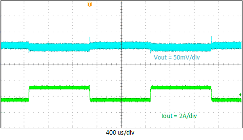 Figure 9-9 Transient Load Response,
Iout = 1.5 to 3 A
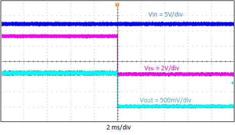 Figure 9-11 Shutdown Relative to
EN
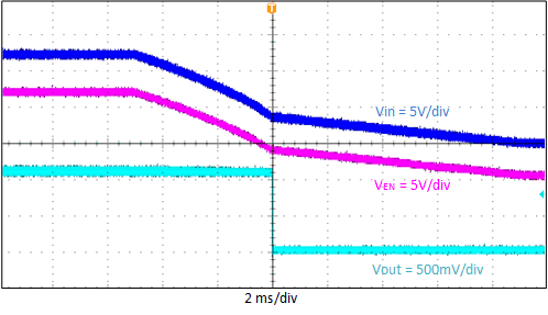 Figure 9-13 Shutdown Relative to
VIN