JAJSJ68B May   2020  – December 2023 TPS566231 , TPS566238

PRODUCTION DATA  

  1.   1
  2. 特長
  3. アプリケーション
  4. 概要
  5. Pin Configuration and Functions
  6. Specifications
    1. 5.1 Absolute Maximum Ratings
    2. 5.2 ESD Ratings
    3. 5.3 Recommended Operating Conditions
    4. 5.4 Thermal Information
    5. 5.5 Electrical Characteristics
    6. 5.6 Typical Characteristics
  7. Detailed Description
    1. 6.1 Overview
    2. 6.2 Functional Block Diagram
    3. 6.3 Feature Description
      1. 6.3.1 PWM Operation and D-CAP3™ Control Mode
      2. 6.3.2 Soft Start
      3. 6.3.3 Power Good
      4. 6.3.4 Large Duty Operation
      5. 6.3.5 Overcurrent Protection and Undervoltage Protection
      6. 6.3.6 Overvoltage Protection
      7. 6.3.7 UVLO Protection
      8. 6.3.8 Output Voltage Discharge
      9. 6.3.9 Thermal Shutdown
    4. 6.4 Device Functional Modes
      1. 6.4.1 Advanced Eco-mode Control
      2. 6.4.2 Force CCM Mode
      3. 6.4.3 Standby Operation
  8. Application and Implementation
    1. 7.1 Application Information
    2. 7.2 Typical Application
      1. 7.2.1 Design Requirements
      2. 7.2.2 Detailed Design Procedure
        1. 7.2.2.1 Custom Design with WEBENCH® Tools
        2. 7.2.2.2 Output Voltage Setpoint
        3. 7.2.2.3 Inductor Selection
        4. 7.2.2.4 Output Capacitor Selection
        5. 7.2.2.5 Input Capacitor Selection
      3. 7.2.3 Application Curves
    3. 7.3 Power Supply Recommendations
    4. 7.4 Layout
      1. 7.4.1 Layout Guidelines
      2. 7.4.2 Layout Example
  9. Device and Documentation Support
    1. 8.1 Device Support
      1. 8.1.1 Development Support
        1. 8.1.1.1 Custom Design with WEBENCH® Tools
    2. 8.2 ドキュメントの更新通知を受け取る方法
    3. 8.3 サポート・リソース
    4. 8.4 Trademarks
    5. 8.5 静電気放電に関する注意事項
    6. 8.6 用語集
  10. Revision History
  11. 10Mechanical, Packaging, and Orderable Information

パッケージ・オプション

メカニカル・データ(パッケージ|ピン)
サーマルパッド・メカニカル・データ
発注情報

Typical Characteristics

GUID-A1309372-C20F-4937-9BE3-8912728A9EE1-low.gif
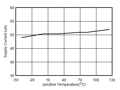
VEN = 5 V TPS566231
Figure 5-1 Supply Current vs Junction Temperature
GUID-C82ECF3B-CA9D-4BC2-9BFA-189998D51890-low.gif
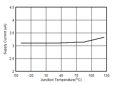
VEN = 0 V 
Figure 5-3 Shutdown Current vs Temperature
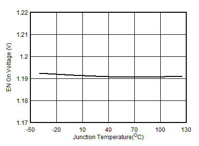
GUID-20201130-CA0I-WN2S-5FGS-RH44RP57FXVP-low.gifFigure 5-5 Enable-On Voltage vs Junction Temperature
GUID-547C0BFB-E4BE-4F55-907D-4954BA06E87B-low.gif
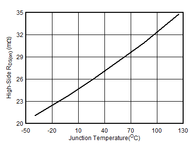
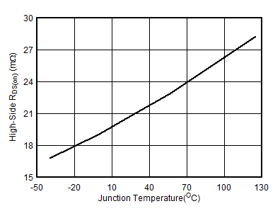
VIN = 12 V
Figure 5-7 High-Side RDS(on) vs Junction Temperature
GUID-74FBFD2A-1648-4782-984B-0141C90F0DB1-low.gif
VIN = 3 V
Figure 5-9 High-Side RDS(on) vs Junction Temperature
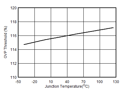
GUID-20201130-CA0I-GSJC-KR3L-FNJVFRHHJGGG-low.gifFigure 5-11 OVP Threshold vs Junction Temperature
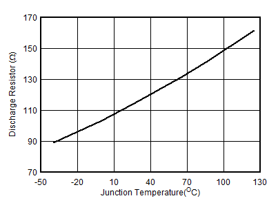
GUID-4E21E2A6-A953-42D7-94F2-EBD4FEC24715-low.gifFigure 5-13 Discharge Resistor vs Junction Temperature
GUID-20201130-CA0I-1DRG-GPVC-BRZMX2GHBPP6-low.gif
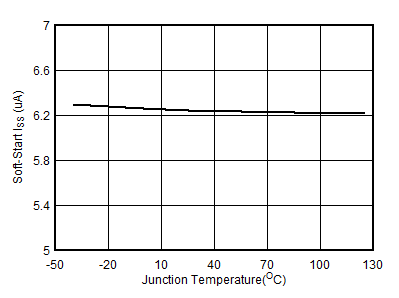
TPS566231 and TPS566238
Figure 5-15 Soft-Start Charge Current Iss vs Junction Temperature
GUID-20201207-CA0I-TKT3-NRVW-TJPPD3XZCRBD-low.gif
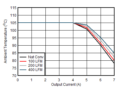
VIN = 12 V VOUT = 1.0 V
Figure 5-17 Safe Operating Area
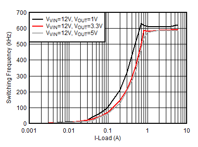
GUID-49082FE9-55F2-4AD9-9D62-45A6F8DB1DD1-low.gifFigure 5-19 TPS566231 and TPS566231P
FSW Load Regulation
GUID-ACD9C982-D744-4825-8CA9-0E0CAD46343B-low.gif
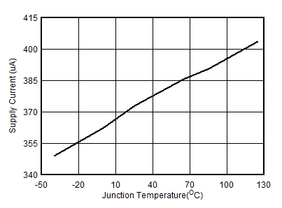
VEN = 5 V TPS566238
Figure 5-2 Supply Current vs Junction Temperature
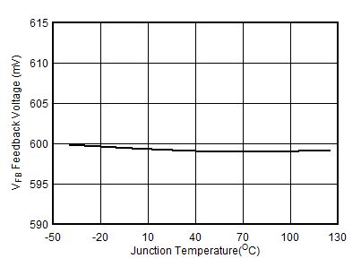
GUID-20201130-CA0I-F3KJ-CB0R-WSJM076KSGML-low.gifFigure 5-4 Feedback Voltage vs Junction Temperature
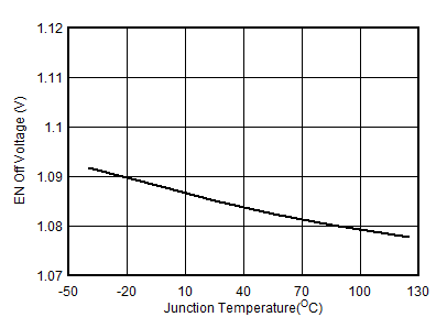
GUID-20201130-CA0I-MC2K-3D3G-L9QNQ2QTFBNB-low.gifFigure 5-6 Enable-Off Voltage vs Junction Temperature
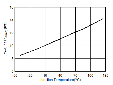
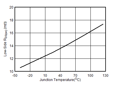
GUID-20011E4F-09F0-4285-B20B-8F3D21211699-low.gif
VIN = 12 V
Figure 5-8 Low-Side RDS(on) vs Junction Temperature
GUID-8E48A1B8-4716-4800-B756-048A059B382A-low.gif
VIN = 3 V
Figure 5-10 Low-Side RDS(on) vs Junction Temperature
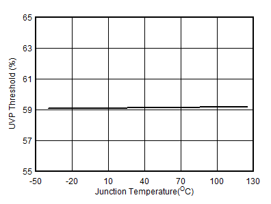
GUID-20201130-CA0I-VQMX-FBL5-8V10LTHZWZPT-low.gifFigure 5-12 UVP Threshold vs Junction Temperature
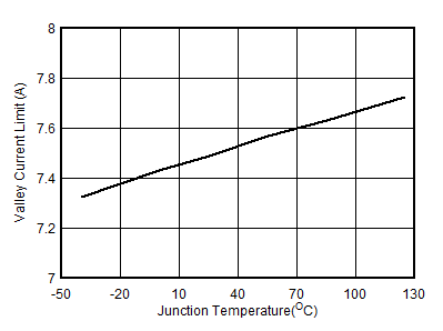
GUID-20201130-CA0I-8KLJ-RV9Q-DHSTPSZJSMND-low.gifFigure 5-14 Valley Current Limit vs Junction Temperature
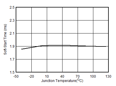
GUID-20201130-CA0I-D62F-F4WK-5PSKM1KNNR6W-low.gif
TPS566231P and TPS566238P
Figure 5-16 Soft-Start Time vs Junction Temperature
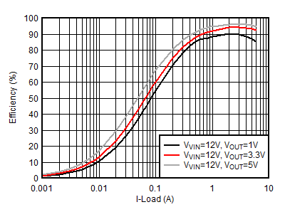
GUID-AD20EA22-0B20-4250-9AD4-7B483C13832E-low.gif
VIN = 12 V
Figure 5-18 TPS566238 and TPS566238P Efficiency
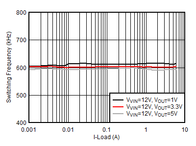
GUID-C4B7FFDD-324B-4C87-A602-E6851BB4CC99-low.gifFigure 5-20 TPS566238 and TPS566238P
FSW Load Regulation