JAJSJ68B May 2020 – December 2023 TPS566231 , TPS566238
PRODUCTION DATA
- 1
- 1 特長
- 2 アプリケーション
- 3 概要
- 4 Pin Configuration and Functions
- 5 Specifications
- 6 Detailed Description
- 7 Application and Implementation
- 8 Device and Documentation Support
- 9 Revision History
- 10Mechanical, Packaging, and Orderable Information
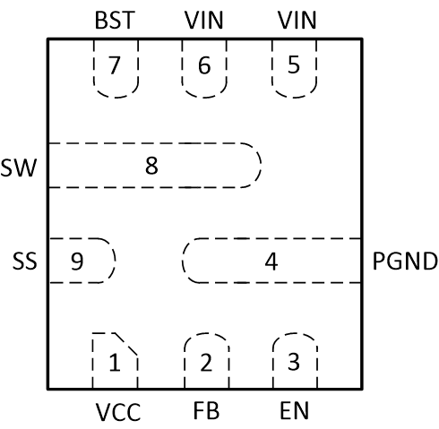
4 Pin Configuration and Functions
 Figure 4-1 TPS566231, TPS566238 9-Pin
 RQF, VQFN-HR Package (Top View)
 Figure 4-2 TPS566231P, TPS566238P 9-Pin
 RQF, VQFN-HR Package (Top View)
Table 4-1 Pin Functions
| PIN | TYPE | DESCRIPTION | |
|---|---|---|---|
| NAME | NO. | ||
| VCC | 1 | O | 5.0-V internal VCC LDO output. This pin supplies voltage to the internal circuitry and gate driver. Bypass this pin with a 1-μF capacitor. If VVIN is lower than 5 V, VCC follows the VIN voltage. |
| FB | 2 | I | Converter feedback input. Connect to the center tap of the resistor divider between output voltage and ground. |
| EN | 3 | I | Enable pin of buck converter. The EN pin is a digital input pin, so the pin decides to turn on or turn off the buck converter. If the EN pin is open, the internal pullup current occurs to enable converter. |
| PGND | 4 | G | Ground pin. Power ground return for the switching circuit. Connect sensitive SS and FB returns to PGND at a single point. |
| VIN | 5, 6 | P | Input voltage supply pin. Connect the input decoupling capacitors between VIN and PGND. |
| BST | 7 | O | Supply input for the gate drive voltage of the high-side MOSFET. Connect the bootstrap capacitor between BST and SW. TI recommends 0.1 μF. |
| SW | 8 | O | Switch node terminal. Connect the output inductor to this pin. |
| SS/PG | 9 | O | TPS566231 and TPS566238 soft-start control pin. Connecting an external capacitor sets the soft-start time. |
| O | TPS566231P and TPS566238P open-drain power good indicator. This pin is asserted low if output voltage is out of PG threshold, over voltage, or if the device is under thermal shutdown, EN shutdown, or during soft start. | ||