JAJSCL3C October   2016  – August 2023 TPS568215

PRODUCTION DATA  

  1.   1
  2. 特長
  3. アプリケーション
  4. 概要
  5. Revision History
  6. Pin Configuration and Functions
  7. Specifications
    1. 6.1 Absolute Maximum Ratings
    2. 6.2 ESD Ratings
    3. 6.3 Recommended Operating Conditions
    4. 6.4 Thermal Information
    5. 6.5 Electrical Characteristics
    6. 6.6 Timing Requirements
    7. 6.7 Typical Characteristics
  8. Detailed Description
    1. 7.1 Overview
    2. 7.2 Functional Block Diagram
    3. 7.3 Feature Description
      1. 7.3.1  PWM Operation and D-CAP3 Control Mode
      2. 7.3.2  Eco-mode Control
      3. 7.3.3  4.7 V LDO and External Bias
      4. 7.3.4  MODE Selection
      5. 7.3.5  Soft Start and Pre-biased Soft Start
      6. 7.3.6  Enable and Adjustable UVLO
      7. 7.3.7  Power Good
      8. 7.3.8  Overcurrent Protection and Undervoltage Protection
      9. 7.3.9  Out-of-Bounds Operation
      10. 7.3.10 UVLO Protection
      11. 7.3.11 Thermal Shutdown
      12. 7.3.12 Output Voltage Discharge
    4. 7.4 Device Functional Modes
      1. 7.4.1 Light Load Operation
      2. 7.4.2 Standby Operation
  9. Application and Implementation
    1. 8.1 Application Information
    2. 8.2 Typical Application
      1. 8.2.1 Design Requirements
      2. 8.2.2 Detailed Design Procedure
        1. 8.2.2.1 External Component Selection
          1. 8.2.2.1.1 Output Voltage Set Point
          2. 8.2.2.1.2 Switching Frequency and Mode Selection
          3. 8.2.2.1.3 Inductor Selection
          4. 8.2.2.1.4 Output Capacitor Selection
          5. 8.2.2.1.5 Input Capacitor Selection
      3. 8.2.3 Application Curves
    3. 8.3 Power Supply Recommendations
    4. 8.4 Layout
      1. 8.4.1 Layout Guidelines
      2. 8.4.2 Layout Example
  10. Device and Documentation Support
    1. 9.1 Device Support
      1. 9.1.1 サード・パーティ製品に関する免責事項
      2. 9.1.2 Development Support
    2. 9.2 ドキュメントの更新通知を受け取る方法
    3. 9.3 サポート・リソース
    4. 9.4 Trademarks
    5. 9.5 静電気放電に関する注意事項
    6. 9.6 用語集
  11. 10Mechanical, Packaging, and Orderable Information

パッケージ・オプション

メカニカル・データ(パッケージ|ピン)
サーマルパッド・メカニカル・データ
発注情報

Application Curves

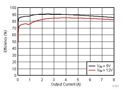
Figure 8-2 through Figure 8-18 apply to the circuit of Figure 8-1. VIN = 12 V. Ta = 25 °C unless otherwise specified.
GUID-39317ED0-A689-4166-8342-9C6E11D4EEDC-low.gif
Figure 8-2 Efficiency
GUID-230949FF-F16A-41B6-A8AB-8B902C609A78-low.gif
Figure 8-3 Light Load Efficiency
GUID-A6D19FDE-0D6F-4B18-BF12-32CA51DA8D76-low.gif
Figure 8-4 Load Regulation, VIN = 5 V
GUID-6509F320-FD6F-4306-8AA3-77DB131F8955-low.gif
Figure 8-6 Line Regulation, IOUT = 6 A
GUID-A0DF8BC0-43A7-4918-93D7-D27DCB00E214-low.gif
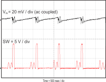
Figure 8-8 Input Voltage Ripple, IOUT = 10 mA
GUID-72A26274-9720-4C5E-8045-A5498811D17C-low.gif
Figure 8-10 Input Voltage Ripple, IOUT = 8 A
GUID-23EF1F3A-B4F2-4388-8811-410983403207-low.gif
Figure 8-12 Output Voltage Ripple, IOUT = 700 mA
GUID-C6F7D036-8FED-4DAC-A39A-62AC1998A35E-low.gif
Figure 8-14 Start Up Relative to VIN Rising
GUID-731CA011-26AB-4DE7-B372-09BB1CDD217E-low.gif
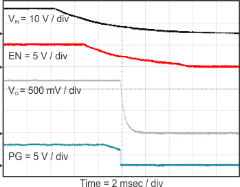
Figure 8-16 Shut Down Relative to VIN Falling
GUID-9B789E39-38C7-4F0B-A594-C030CF45E60C-low.gif
Figure 8-18 Transient Response
GUID-E3E32873-A78E-49C7-A958-387A6D64BC8D-low.gif
Figure 8-5 Load Regulation, VIN = 12 V
GUID-D0621D9D-6106-4CE7-98CA-3C55C5F41A43-low.gif
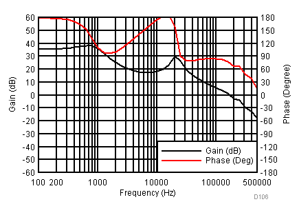
Figure 8-7 Loop Response, IOUT = 6 A
GUID-D57FCC92-BFAD-4950-85AC-B99258CB721B-low.gif
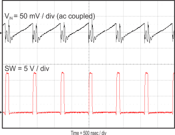
Figure 8-9 Input Voltage Ripple, IOUT = 700 mA
GUID-9D3D8043-9C1D-427E-92DA-D4F0EACFBBFB-low.gif
Figure 8-11 Output Voltage Ripple, IOUT = 10 mA
GUID-268455E5-56F1-4EEB-9306-FEBB4E5E5910-low.gif
Figure 8-13 Output Voltage Ripple, IOUT = 8 A
GUID-7DD9BF94-FFFC-4C4B-9E3C-4BFCC7EF16E5-low.gif
Figure 8-15 Start Up Relative to EN Rising
GUID-E2837383-098D-41A4-92A9-0F4CD1C18767-low.gif
Figure 8-17 Shut Down Relative to EN Falling