JAJSCL3C October 2016 – August 2023 TPS568215
PRODUCTION DATA
- 1
- 1 特長
- 2 アプリケーション
- 3 概要
- 4 Revision History
- 5 Pin Configuration and Functions
- 6 Specifications
-
7 Detailed Description
- 7.1 Overview
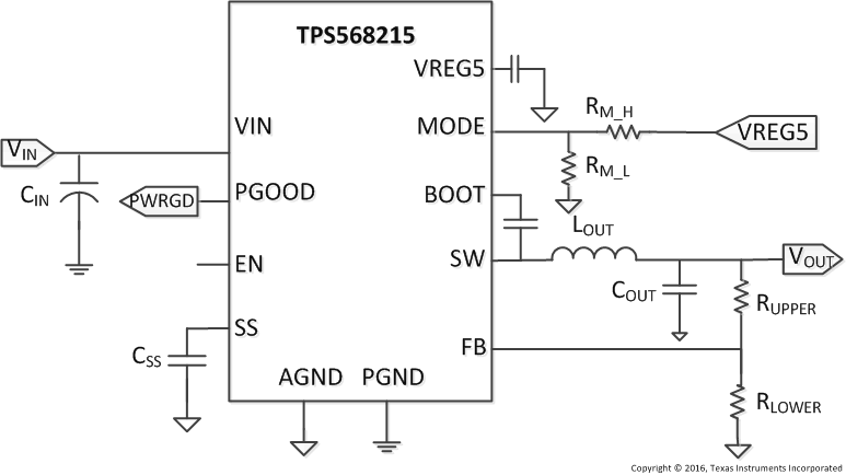
- 7.2 Functional Block Diagram
- 7.3
Feature Description
- 7.3.1 PWM Operation and D-CAP3 Control Mode
- 7.3.2 Eco-mode Control
- 7.3.3 4.7 V LDO and External Bias
- 7.3.4 MODE Selection
- 7.3.5 Soft Start and Pre-biased Soft Start
- 7.3.6 Enable and Adjustable UVLO
- 7.3.7 Power Good
- 7.3.8 Overcurrent Protection and Undervoltage Protection
- 7.3.9 Out-of-Bounds Operation
- 7.3.10 UVLO Protection
- 7.3.11 Thermal Shutdown
- 7.3.12 Output Voltage Discharge
- 7.4 Device Functional Modes
- 8 Application and Implementation
- 9 Device and Documentation Support
- 10Mechanical, Packaging, and Orderable Information
3 概要
TPS568215 はテキサス・インスツルメンツで最小のモノリシック、8A 同期整流降圧型コンバータで、アダプティブ・オンタイム D-CAP3™ 制御モードが搭載されています。このデバイスは、低 RDS(on) のパワー MOSFET を内蔵して高効率を実現し、外付け部品数が最小になるため、スペースの制約が厳しい電力システムでも使いやすくなっています。主要な機能として、非常に正確な基準電圧、高速負荷過渡応答、自動スキップ・モードの動作による軽負荷時の高効率、可変の電流制限、外部補償が不要なことが挙げられます。強制連続導通モードにより、高性能 DSP や FPGA に求められる厳しい電圧レギュレーション精度要件を満たすことができます。TPS568215 は放熱特性の優れた 18 ピン HotRod QFN パッケージで供給され、–40℃~150℃の接合部温度で動作するよう設計されています。TPS568215 は TPS56C215 とピン互換性があり、同じ占有面積で 6A~12A のソリューションを柔軟に選択できます。
パッケージ情報
| 部品番号 | パッケージ (1) | 本体サイズ (公称) |
|---|---|---|
| TPS568215 | RNN (VQFN、18) | 3.5mm × 3.5mm |
(1) 利用可能なすべてのパッケージについては、データシートの末尾にある注文情報を参照してください。