JAJSCX3 January 2017 TPS568215OA
PRODUCTION DATA.
- 1 特長
- 2 アプリケーション
- 3 概要
- 4 改訂履歴
- 5 Pin Configuration and Functions
- 6 Specifications
-
7 Detailed Description
- 7.1 Overview
- 7.2 Functional Block Diagram
- 7.3
Feature Description
- 7.3.1 PWM Operation and D-CAP3 Control
- 7.3.2 Out-of-Audio Operation
- 7.3.3 4.7 V LDO and External Bias
- 7.3.4 MODE Selection
- 7.3.5 Soft Start and Pre-biased Soft Start
- 7.3.6 Enable and Adjustable UVLO
- 7.3.7 Power Good
- 7.3.8 Over Current Protection and Under Voltage Protection
- 7.3.9 Out-of-Bounds Operation
- 7.3.10 UVLO Protection
- 7.3.11 Thermal Shutdown
- 7.3.12 Output Voltage Discharge
- 7.4 Device Functional Modes
- 8 Application and Implementation
- 9 Power Supply Recommendations
- 10Layout
- 11デバイスおよびドキュメントのサポート
- 12メカニカル、パッケージ、および注文情報
6 Specifications
6.1 Absolute Maximum Ratings
over operating free-air temperature range (unless otherwise noted) (1)| MIN | MAX | UNIT | ||
|---|---|---|---|---|
| Input Voltage | VIN | –0.3 | 20 | V |
| SW | –2 | 19 | ||
| SW(10 ns transient) | –3 | 20 | ||
| EN | –0.3 | 6.5 | ||
| BOOT –SW | –0.3 | 6.5 | ||
| BOOT | –0.3 | 25.5 | ||
| SS, MODE, FB | –0.3 | 6.5 | ||
| VREG5 | –0.3 | 6 | ||
| Output Voltage | PGOOD | –0.3 | 6.5 | V |
| Output Current, IOUT(2) | 10 | A | ||
| Operating junction temperature, TJ | –40 | 150 | °C | |
| Storage temperature, Tstg | –55 | 150 | °C | |
(1) Stresses beyond those listed under Absolute Maximum Ratings may cause permanent damage to the device. These are stress ratings only, which do not imply functional operation of the device at these or any other conditions beyond those indicated under Recommended Operating Conditions. Exposure to absolute-maximum-rated conditions for extended periods may affect device reliability.
(2) In order to be consistent with the TI reliability requirement of 100k continuos Power-On-Hours with 105°C junction temperature at the max output current of 10A, the converter's duty cycle should be limited to 60% operation as to prevent electromigration failure in the solder. If higher duty cycle is required at 10A load the total power on hours or the junction temperature have to be reduced.
6.2 ESD Ratings
| VALUE | UNIT | |||
|---|---|---|---|---|
| V(ESD) | Electrostatic discharge | Human-body model (HBM), per ANSI/ESDA/JEDEC JS-001(1) | ±2000 | V |
| Charged-device model (CDM), per JEDEC specification JESD22-C101(2) | ±500 | |||
(1) JEDEC document JEP155 states that 500-V HBM allows safe manufacturing with a standard ESD control process.
(2) JEDEC document JEP157 states that 250-V CDM allows safe manufacturing with a standard ESD control process.
6.3 Recommended Operating Conditions
over operating free-air temperature range (unless otherwise noted)| MIN | NOM | MAX | UNIT | |||
|---|---|---|---|---|---|---|
| Input Voltage | VIN | 4.5 | 17 | V | ||
| SW | –1.8 | 17 | ||||
| BOOT | –0.1 | 23.5 | ||||
| VREG5 | –0.1 | 5.2 | ||||
| TJ | Operating junction temperature | -40 | 150 | °C | ||
6.4 Thermal Information
| THERMAL METRIC(1) | TPS568215OA | UNIT | |
|---|---|---|---|
| RNN (VQFN) | |||
| 18 PINS | |||
| RθJA | Junction-to-ambient thermal resistance | 42.3 | °C/W |
| RθJC(top) | Junction-to-case (top) thermal resistance | 23.9 | °C/W |
| RθJB | Junction-to-board thermal resistance | 10.0 | °C/W |
| ψJT | Junction-to-top characterization parameter | 0.5 | °C/W |
| ψJB | Junction-to-board characterization parameter | 10.0 | °C/W |
| RθJC(bot) | Junction-to-case (bottom) thermal resistance | 0.5 | °C/W |
(1) For more information about traditional and new thermal metrics, see the Semiconductor and IC Package Thermal Metrics application report.
6.5 Electrical Characteristics
TJ = –40°C to 150°C, VIN=12V (unless otherwise noted)| PARAMETER | CONDITIONS | MIN | TYP | MAX | UNIT | |
|---|---|---|---|---|---|---|
| SUPPLY CURRENT | ||||||
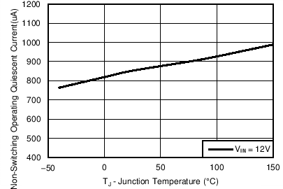
| IIN | VIN supply current | TJ = 25°C, VEN=5 V, non switching | 850 | µA | ||
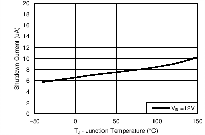
| IVINSDN | VIN shutdown current | TJ = 25°C, VEN=0 V | 7 | µA | ||
| LOGIC THRESHOLD | ||||||
| VENH | EN H-level threshold voltage | 1.175 | 1.225 | 1.3 | V | |
| VENL | EN L-level threshold voltage | 1.025 | 1.104 | 1.15 | V | |
| VENHYS | 0.121 | V | ||||
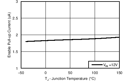
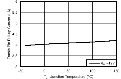
| IENp1 | EN pull-up current | VEN = 1.0 V | 0.35 | 1.91 | 2.95 | µA |
| IENp2 | VEN = 1.3 V | 3 | 4.197 | 5.5 | µA | |
| FEEDBACK VOLTAGE | ||||||
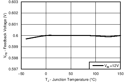
| VFB | FB voltage | TJ = 25°C | 598 | 600 | 602 | mV |
| TJ = 0°C to 85°C | 597.5 | 600 | 602.5 | mV | ||
| TJ = –40°C to 85°C | 594 | 600 | 602.5 | mV | ||
| TJ = –40°C to 150°C | 594 | 600 | 606 | mV | ||
| LDO VOLTAGE | ||||||
| VREG5 | LDO Output voltage | TJ = –40°C to 150°C | 4.58 | 4.7 | 4.83 | V |
| ILIM5 | LDO Output Current limit | TJ = –40°C to 150°C | 100 | 150 | 200 | mA |
| MOSFET | ||||||
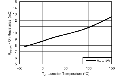
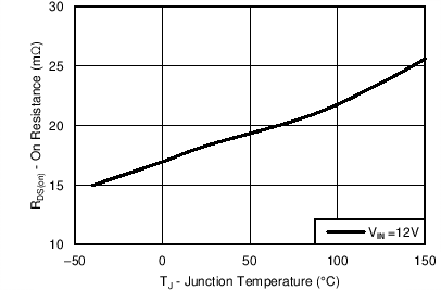
| RDS(on)H | High side switch resistance | TJ = 25°C, VVREG5 = 4.7 V | 19 | mΩ | ||
| RDS(on)L | Low side switch resistance | TJ = 25°C, VVREG5 = 4.7 V | 9.4 | mΩ | ||
| SOFT START | ||||||
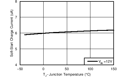
| Iss | Soft start charge current | TJ = -40°C to 150°C | 4.9 | 6 | 7.1 | µA |
| CURRENT LIMIT | ||||||
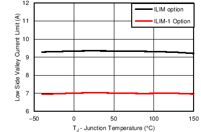
| IOCL | Current Limit (Low side sourcing) | ILIM-1 option, Valley Current | 6 | 7.1 | 8.15 | A |
| ILIM option, Valley Current | 8 | 9.4 | 10.8 | A | ||
| ILIM+1 option, Valley Current | 10 | 11.8 | 13.5 | A | ||
| Current Limit (Low side negative) | Valley Current | 3 | A | |||
| POWER GOOD | ||||||
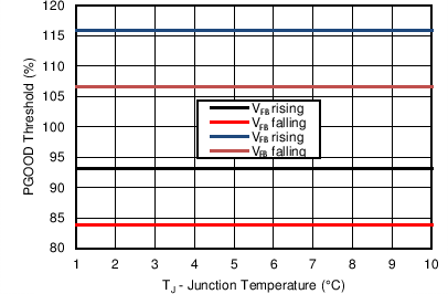
| VPGOODTH | PGOOD threshold | VFB falling (fault) | 84% | %VREF | ||
| VFB rising (good) | 93% | %VREF | ||||
| VFB rising (fault) | 116% | %VREF | ||||
| VFB falling (good) | 107% | %VREF | ||||
| OUTPUT UNDERVOLTAGE PROTECTION | ||||||
| VUVP | Output UVP threshold | Hiccup detect | 68% x VFB | |||
| THERMAL SHUTDOWN | ||||||
| TSDN | Thermal shutdown threshold | Shutdown temperature | 160 | °C | ||
| Hysteresis | 15 | °C | ||||
| TSDN VREG5 | VREG5 thermal shutdown threshold | Shutdown temperature | 171 | °C | ||
| Hysteresis | 18 | °C | ||||
| UVLO | ||||||
| UVLO | UVLO threshold | VREG5 rising voltage | 4.1 | 4.3 | 4.5 | V |
| VREG5 falling voltage | 3.34 | 3.57 | 3.8 | V | ||
| VREG5 hysteresis | 730 | mV | ||||
6.6 Timing Requirements
| PARAMETER | CONDITIONS | MIN | TYP | MAX | UNIT | |
|---|---|---|---|---|---|---|
| ON-TIME TIMER CONTROL | ||||||
| tON | SW On Time | VIN = 12 V, VOUT=3.3 V, FSW = 800 kHz | 310 | 340 | 380 | ns |
| tON min | SW Minimum on time | VIN = 17 V, VOUT=0.6 V, FSW= 1200 kHz | 54 | ns | ||
| tOFF | SW Minimum off time | 25°C, VFB=0.5 V | 310 | ns | ||
| FSWOOA | OOA Switching Frequency | TJ = -40°C to 150°C, No Load | 20 | 27 | KHz | |
| SOFT START | ||||||
| tSS | Soft start time | Internal soft start time | 1.045 | ms | ||
| OUTPUT UNDERVOLTAGE AND OVERVOLTAGE PROTECTION | ||||||
| tUVPDEL | Output Hiccup delay relative to SS time | UVP detect | 1 | cycle | ||
| tUVPEN | Output Hiccup enable delay relative to SS time | UVP detect | 7 | cycle | ||
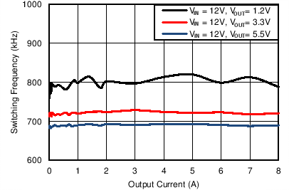
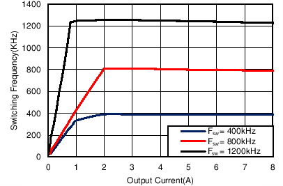
6.7 Typical Characteristics
