JAJSGE5C March 2019 – August 2019 TPS568230
PRODUCTION DATA.
- 1 特長
- 2 アプリケーション
- 3 概要
- 4 改訂履歴
- 5 概要(続き)
- 6 Pin Configuration and Functions
- 7 Specifications
- 8 Detailed Description
- 9 Application and Implementation
- 10Power Supply Recommendations
- 11Layout
- 12デバイスおよびドキュメントのサポート
- 13メカニカル、パッケージ、および注文情報
7.6 Typical Characteristics
TJ=-40oC to 125oC, VVIN=12V(unless otherwise noted)
| VEN = 3.3 V |

1.
Figure 3. Feedback Voltage vs Junction Temperature 
1.
Figure 5. Enable Off Voltage vs Junction Temperature 
1.
Figure 7. Low-Side RDS(on) vs Junction Temperature 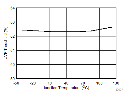
1.
Figure 9. UVP Threshold vs Junction Temperature 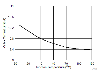
1.
Figure 11. Valley Current Limit vs Junction Temperature 
1.
Figure 13. Efficiency, Eco-mode, FSW = 600 kHz 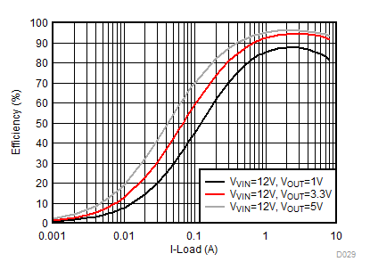
1.
Figure 15. Efficiency, FCCM, FSW = 600 kHz 
1.
Figure 17. Efficiency, OOA-mode, FSW = 1 MHz 
1.
Figure 19. Load Regulation, Eco-mode, FSW = 600 kHz 
1.
Figure 21. FSW Load Regulation, OOA-mode, FSW = 600 kHz 
1.
Figure 23. FSW Load Regulation, Eco-mode, FSW = 800 kHz 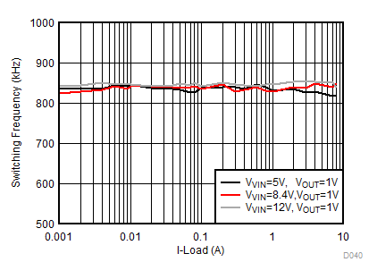
1.
Figure 25. FSW Load Regulation, FCCM, FSW = 800 kHz 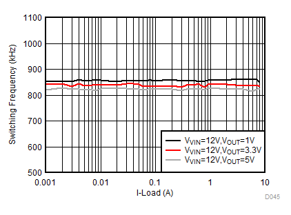
1.
Figure 27. FSW Load Regulation, FCCM, FSW = 800 kHz 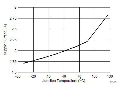
| VEN = 0 V |
1.
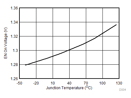
Figure 4. Enable On Voltage vs Junction Temperature 
1.
Figure 6. High-Side RDS(on) vs Junction Temperature 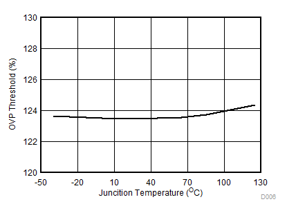
1.
Figure 8. OVP Threshold vs Junction Temperature 
1.
Figure 10. Discharge Resistor vs Junction Temperature 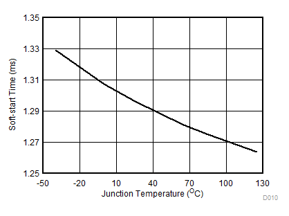
1.
Figure 12. Soft-Start Time vs Junction Temperature 
1.
Figure 14. Efficiency, OOA-mode, FSW = 600 kHz 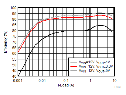
1.
Figure 16. Efficiency, Eco-mode, FSW = 1 MHz 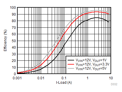
1.
Figure 18. Efficiency, FCCM, FSW = 1 MHz 
1.
Figure 20. FSW Load Regulation, Eco-mode, FSW = 600 kHz 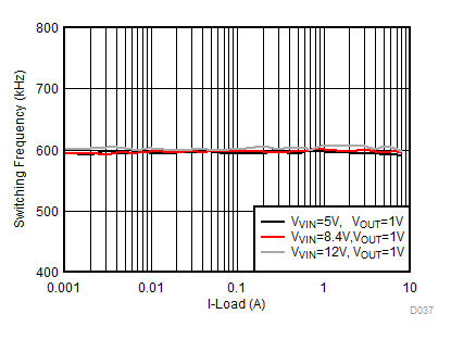
1.
Figure 22. FSW Load Regulation, FCCM, FSW = 600 kHz 
1.
Figure 24. FSW Load Regulation, OOA-mode, FSW = 800 kHz 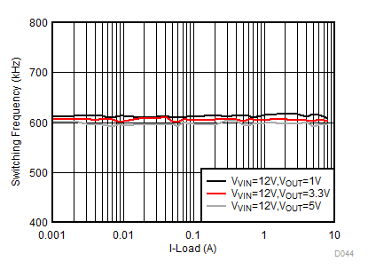
1.
Figure 26. FSW Load Regulation, FCCM, FSW = 600 kHz 
1.
Figure 28. FSW Load Regulation, FCCM, FSW = 1 MHz