SLVS258B November 1999 – December 2016 TPS60130 , TPS60131 , TPS60132 , TPS60133
PRODUCTION DATA.
- 1 Features
- 2 Applications
- 3 Description
- 4 Revision History
- 5 Device Options
- 6 Pin Configuration and Functions
- 7 Specifications
- 8 Parameter Measurement Information
- 9 Detailed Description
- 10Application and Implementation
- 11Power Supply Recommendations
- 12Layout
- 13Device and Documentation Support
- 14Mechanical, Packaging, and Orderable Information
パッケージ・オプション
メカニカル・データ(パッケージ|ピン)
- PWP|20
サーマルパッド・メカニカル・データ
- PWP|20
発注情報
12 Layout
12.1 Layout Guidelines
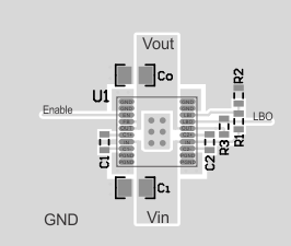
Careful board layout is necessary due to the high transient currents and switching frequency of the converter. All capacitors must be soldered in close proximity to the IC. Connect ground and power ground pins through a short, low-impedance trace. A PCB layout proposal for a two-layer board is given in Figure 33. The bottom layer of the board carries only ground potential for best performance. The layout also provides improved thermal performance as the exposed lead frame is soldered to the PCB.
An evaluation module for the TPS60130 is available and can be ordered under product code TPS60130EVM-143. The EVM uses the layout shown in Figure 33 and components in Table 7.
The best performance of the converter is achieved with the additional bypass capacitors C5 and C6 at input and output. Capacitor C7 must be included if the large line transients are expected. The capacitors are not required. They can be omitted in most applications.
12.2 Layout Example
 Figure 33. Recommended PCB Layout for TPS6013x
Table 7. Component Identification
| COMPONENT | DESCRIPTION |
|---|---|
| IC1 | TPS6013x |
| C1, C2 | Flying capacitors |
| C3, C6 | Input capacitors |
| C4, C5 | Onput capacitors |
| C7 | Stabilization capacitor for LBI |
| R1, R2 | Resistive divider for LBI |
| R3 | Pullup resistor for LBO |
12.3 Power Dissipation
The power dissipated in the TPS6013x depends on output current and the mode of operation (1.5× or doubler voltage conversion mode). It is described by Equation 5.

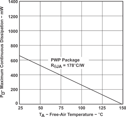
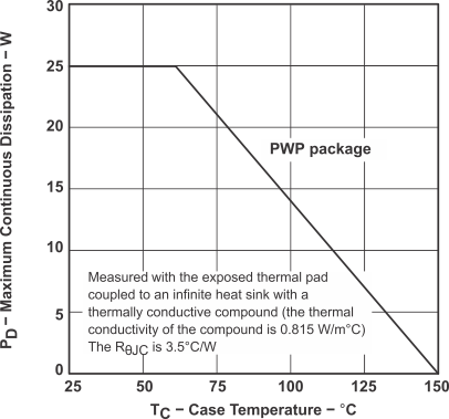
PDISS must be less than that allowed by the package rating. See Absolute Maximum Ratings for 20-pin PWP package power-dissipation limits and deratings.
 Figure 34. Dissipation Derating Curves
vs Free-Air Temperature
 Figure 35. Maximum Continuous Dissipation
vs Case Temperature