SLVS274A March 2000 – April 2016 TPS60200 , TPS60201 , TPS60202 , TPS60203
PRODUCTION DATA.
- 1 Features
- 2 Applications
- 3 Description
- 4 Revision History
- 5 Device Comparison Tables
- 6 Pin Configuration and Functions
- 7 Specifications
- 8 Detailed Description
- 9 Application and Implementation
- 10Power Supply Recommendations
- 11Layout
- 12Device and Documentation Support
- 13Mechanical, Packaging, and Orderable Information
1 Features
- Regulated 3.3-V Output Voltage With up to
100-mA Output Current From a 1.8-V to 3.6-V Input Voltage - Less Than 5-mV (PP) Output Voltage Ripple Achieved With Push-Pull Topology
- Integrated Low-Battery and Power-Good Detector
- Switching Frequency Can Be Synchronized to External Clock Signal
- Extends Battery Usage With up to 90% Efficiency and 35-μA Quiescent Supply Current
- Reliable System Shutdown Because Output Capacitor Is Discharged When Device Is Disabled
- Easy-to-Design, Low-Cost, Low-EMI Power Supply Since No Inductors Are Used
- 0.05-μA Shutdown Current, Battery Is Isolated From Load in Shutdown Mode
- Compact Converter Solution in UltraSmall 10-pin MSOP With Only Four External Capacitors Required
- Evaluation Module Available (TPS60200EVM-145)
2 Applications
- Two Battery Cells to 3.3-V Conversion
- MP3 Portable Audio Players
- Battery-Powered Microprocessor Systems
- Backup-Battery Boost Converters
- PDAs, Organizers, and Cordless Phones
- Handheld Instrumentation
- Glucose Meters and Other Medical Instruments
3 Description
The TPS6020x step-up, regulated charge pumps generate a 3.3-V ±4% output voltage from a 1.8-V to 3.6-V input voltage. The devices are typically powered by two Alkaline, NiCd or NiMH battery cells and operate down to a minimum supply voltage of
1.6 V. Continuous output current is a minimum of 100 mA for the TPS60200 and TPS60201 and 50 mA for the TPS60202 and TPS60203, all from a 2-V input. Only four external capacitors are needed to build a complete low-ripple DC/DC converter. The push-pull operating mode of two single-ended charge pumps assures the low output voltage ripple as current is continuously transferred to the output.
Device Information(1)
| PART NUMBER | PACKAGE | BODY SIZE (NOM) |
|---|---|---|
| TPS6020x | MSOP (10) | 3.00 mm × 3.00 mm |
- For all available packages, see the orderable addendum at the end of the data sheet.
spacer
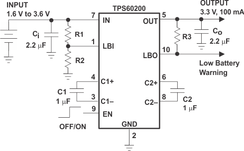
Typical Application with Low-Battery Warning |
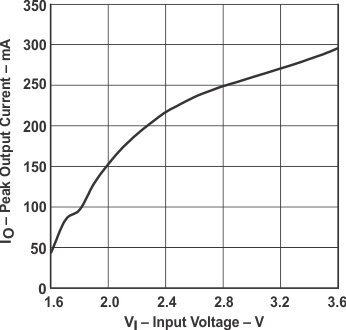
TPS60200 Peak Output Current |
|
 |
||
 |
||