SLVS391C October   2001  – September 2015 TPS60500 , TPS60501 , TPS60502 , TPS60503

PRODUCTION DATA.  

  1. Features
  2. Applications
  3. Description
  4. Revision History
  5. Device Comparison Table
  6. Pin Configuration and Functions
  7. Specifications
    1. 7.1 Absolute Maximum Ratings
    2. 7.2 ESD Ratings
    3. 7.3 Recommended Operating Conditions
    4. 7.4 Thermal Information
    5. 7.5 Electrical Characteristics
    6. 7.6 Typical Characteristics
  8. Detailed Description
    1. 8.1 Overview
    2. 8.2 Functional Block Diagram
    3. 8.3 Feature Description
      1. 8.3.1 Short-Circuit Current Limit and Thermal Protection
      2. 8.3.2 Enable
      3. 8.3.3 Power Good Detector
    4. 8.4 Device Functional Modes
      1. 8.4.1 Start-up Procedure
      2. 8.4.2 Conversion Modes
        1. 8.4.2.1 LDO Conversion Mode
        2. 8.4.2.2 2/3x Conversion Mode
        3. 8.4.2.3 0.5x Conversion Mode
        4. 8.4.2.4 1/3x Conversion Mode
  9. Application and Implementation
    1. 9.1 Application Information
    2. 9.2 Typical Applications
      1. 9.2.1 Typical Application Circuit for Fixed-Voltage and Adjustable-Voltage Versions
        1. 9.2.1.1 Design Requirements
        2. 9.2.1.2 Detailed Design Procedure
          1. 9.2.1.2.1 Capacitor Selection
          2. 9.2.1.2.2 Resistor Combinations
        3. 9.2.1.3 Application Curves
    3. 9.3 System Examples
      1. 9.3.1 DSP Supply With Sequencing
      2. 9.3.2 LC-Post Filter
      3. 9.3.3 Power Supply With Dynamic Voltage Scaling
      4. 9.3.4 Internet Audio Power Supply
  10. 10Power Supply Recommendations
  11. 11Layout
    1. 11.1 Layout Guidelines
    2. 11.2 Layout Examples
  12. 12Device and Documentation Support
    1. 12.1 Device Support
      1. 12.1.1 Third-Party Products Disclaimer
    2. 12.2 Related Links
    3. 12.3 Community Resources
    4. 12.4 Trademarks
    5. 12.5 Electrostatic Discharge Caution
    6. 12.6 Glossary
  13. 13Mechanical, Packaging, and Orderable Information

パッケージ・オプション

メカニカル・データ(パッケージ|ピン)
サーマルパッド・メカニカル・データ
発注情報

6 Pin Configuration and Functions

DGS Package
10-Pin VSSOP
Top View
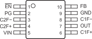
TPS60500 TPS60501 TPS60502 TPS60503 pinout1.gif

Pin Functions

PIN I/O DESCRIPTION
NAME NO.
C1F+ 6 Positive terminal of the flying capacitor C1F
C1F− 8 Negative terminal of the flying capacitor C1F
C2F+ 4 Positive terminal of the flying capacitor C2F
C2F− 3 Negative terminal of the flying capacitor C2F
EN 1 I Device-enable Input.
EN = High disables the device. Output and input are isolated in shutdown mode.
EN = Low enables the device.
GND 9 Ground
FB 10 O TPS60500: connect via voltage divider to VO
TPS60501 to TPS60503: connect directly to VO
OUT 7 O Regulated 3.3 V, 1.8 V, 1.5 V, or adjustable power output
Bypass OUT to GND with the output filter capacitor Co.
PG 2 O Open drain power good detector output. As soon as the voltage on OUT reaches about 97% of its nominal value this pin goes high.
VIN 5 I Supply Input. Connect to an input supply in the 1.8-V to 6.5-V range.