JAJSHY7B September   2019  – August 2020 TPS61023

PRODUCTION DATA  

  1. 特長
  2. アプリケーション
  3. 概要
  4. Revision History
  5. Pin Configuration and Functions
    1.     Pin Functions
  6. Specifications
    1. 6.1 Absolute Maximum Ratings
    2. 6.2 ESD Ratings
    3. 6.3 Recommended Operating Conditions
    4. 6.4 Thermal Information
    5. 6.5 Electrical Characteristics
    6. 6.6 Typical Characteristics
  7. Detailed Description
    1. 7.1 Overview
    2. 7.2 Functional Block Diagram
    3. 7.3 Feature Description
      1. 7.3.1 Undervoltage Lockout
      2. 7.3.2 Enable and Soft Start
      3. 7.3.3 Switching Frequency
      4. 7.3.4 Current Limit Operation
      5. 7.3.5 Pass-Through Operation
      6. 7.3.6 Overvoltage Protection
      7. 7.3.7 Output Short-to-Ground Protection
      8. 7.3.8 Thermal Shutdown
    4. 7.4 Device Functional Modes
      1. 7.4.1 PWM Mode
      2. 7.4.2 Power-Save Mode
  8. Application and Implementation
    1. 8.1 Application Information
    2. 8.2 Typical Application
      1. 8.2.1 Design Requirements
      2. 8.2.2 Detailed Design Procedure
        1. 8.2.2.1 Setting the Output Voltage
        2. 8.2.2.2 Inductor Selection
        3. 8.2.2.3 Output Capacitor Selection
        4. 8.2.2.4 Loop Stability, Feedforward Capacitor Selection
        5. 8.2.2.5 Input Capacitor Selection
      3. 8.2.3 Application Curves
  9. Power Supply Recommendations
  10. 10Layout
    1. 10.1 Layout Guidelines
    2. 10.2 Layout Example
    3. 10.3 Thermal Considerations
  11. 11Device and Documentation Support
    1. 11.1 Device Support
      1. 11.1.1 Third-Party Products Disclaimer
    2. 11.2 Receiving Notification of Documentation Updates
    3. 11.3 Support Resources
    4. 11.4 Trademarks
    5. 11.5 静電気放電に関する注意事項
    6. 11.6 Glossary
  12. 12Mechanical, Packaging, and Orderable Information
    1. 12.1 Package Option Addendum
    2. 12.2 Tape and Reel Information

パッケージ・オプション

メカニカル・データ(パッケージ|ピン)
サーマルパッド・メカニカル・データ

Typical Characteristics

VIN = 3.6 V, VOUT = 5 V, TJ = 25°C, unless otherwise noted
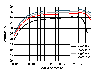
GUID-C68A7FFB-55C6-432F-9145-5A604939637A-low.gif
VIN = 1.8 V, 3.0 V, 3.6 V, 4.2 V; VOUT = 5 V
Figure 6-1 Load Efficiency With Different Input
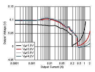
GUID-DE4CFA31-8913-4AB2-9F7B-AA36A7F1CD46-low.gif
VIN = 1.8 V, 3.0 V, 3.6 V, 4.2 V; VOUT = 5 V
Figure 6-3 Load Regulation
GUID-B1ABC36E-550E-48A1-BAFE-6BCDA05C7BD0-low.gif
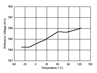
VIN = 3.6 V; VOUT = 5 V, TJ = –40°C to +125°C
Figure 6-5 Reference Voltage vs Temperature
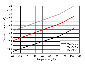
GUID-38DDC701-68E1-42D5-89F1-F404FE58789E-low.gif
VIN = 1.8 V; VOUT = 2.2 V, 3.6 V, 5 V, TJ = –40°C to +125°C, No switching
Figure 6-7 Quiescent Current into VOUT vs Temperature
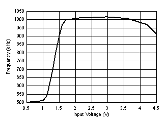
GUID-D4D176F6-5961-4C60-B2BC-D4083F83D80C-low.gif
VIN = 0.5 V to 4.5 V; VOUT = 5 V
Figure 6-9 Switching Frequency vs Input Voltage
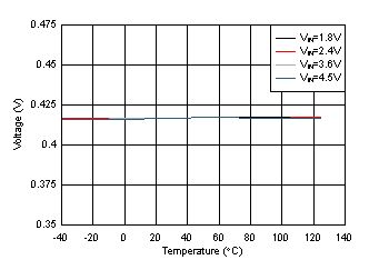
GUID-4C7C439D-2ABD-4C20-99FD-094332E610ED-low.gif
VIN = 1.8 V, 2.4 V, 3.6 V, 4.5 V; VOUT = 0 V; TJ = –40°C to +125°C
Figure 6-11 EN Falling Threshold vs Temperature
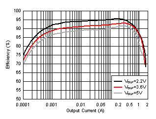
GUID-50DC911F-45AA-414A-8A66-9B3ADBB35572-low.gif
VIN = 1.8 V; VOUT = 2.2 V, 3.6 V, 5 V
Figure 6-2 Load Efficiency With Different Output
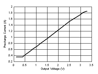
GUID-38E9AE36-6B5E-4D24-9167-19F7766ECABC-low.gif
VIN = 3.6 V; VOUT = 0.1 V to 3.3 V
Figure 6-4 Pre-charge Current vs Output Voltage
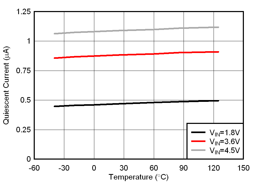
GUID-25A942DB-064F-454B-A70A-38AF905B150E-low.gif
VIN = 1.8 V, 3.6 V 4.5 V; VOUT = 5 V, TJ = –40°C to +125°C, No switching
Figure 6-6 Quiescent Current into VIN vs Temperature
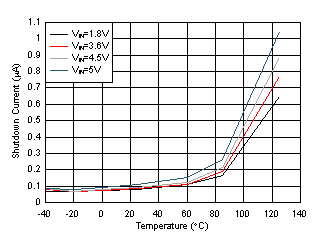
GUID-592FCB5C-51AD-4315-AD3B-30A3D70B034B-low.gif
VIN = VSW = 1.8 V, 3.6 V, 4.5 V, 5 V; VOUT = 0 V; TJ = –40°C to +125°C
Figure 6-8 Shutdown Current vs Temperature
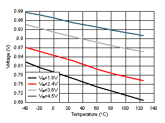
GUID-96CD87D5-5721-40B3-8A71-E71EEA81446B-low.gif
VIN = 1.8 V, 2.4 V, 3.6 V, 4.5 V; VOUT = 0 V; TJ = –40°C to +125°C
Figure 6-10 EN Rising Threshold vs Temperature