JAJSMQ0D October 2022 – September 2023 TPS61033 , TPS610333
PRODUCTION DATA
- 1
- 1 特長
- 2 アプリケーション
- 3 概要
- 4 Device Comparison Table
- 5 Revision History
- 6 Pin Configuration and Functions
- 7 Specifications
-
8 Detailed Description
- 8.1 Overview
- 8.2 Functional Block Diagram
- 8.3
Feature Description
- 8.3.1 Undervoltage Lockout
- 8.3.2 Enable and Soft Start
- 8.3.3 Setting the Output Voltage
- 8.3.4 Current Limit Operation
- 8.3.5 Pass-Through Operation
- 8.3.6 Power Good Indicator
- 8.3.7 Implement Output Discharge by PG function
- 8.3.8 Overvoltage Protection
- 8.3.9 Output Short-to-Ground Protection
- 8.3.10 Thermal Shutdown
- 8.4 Device Functional Modes
- 9 Application and Implementation
- 10Device and Documentation Support
- 11Mechanical, Packaging, and Orderable Information
8.4.2 Power-Save Mode
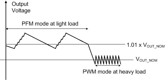
The TPS61033 integrates a power-save mode with PFM to improve efficiency at light load. When the load current decreases, the inductor valley current set by the output of the error amplifier no longer regulates the output voltage. When the inductor valley current hits the low limit, the output voltage exceeds the setting voltage as the load current decreases further. When the FB voltage hits the PFM reference voltage, the TPS61033 goes into the power-save mode. In the power-save mode, when the FB voltage rises and hits the PFM reference voltage, the device continues switching for several cycles because of the delay time of the internal comparator — then it stops switching. The load is supplied by the output capacitor, and the output voltage declines. When the FB voltage falls below the PFM reference voltage, after the delay time of the comparator, the device starts switching again to ramp up the output voltage.
 Figure 8-2 Output Voltage in PWM Mode and PFM Mode