SLUS525A March 2007 – September 2015 TPS61050 , TPS61052
PRODUCTION DATA.
- 1 Features
- 2 Applications
- 3 Description
- 4 Revision History
- 5 Pin Configuration and Functions
- 6 Specifications
- 7 Detailed Description
-
8 Application and Implementation
- 8.1 Application Information
- 8.2
Typical Applications
- 8.2.1 Typical Application Schematic
- 8.2.2 High-Power White LED Solution Featuring Privacy Indicator
- 8.2.3 High-Power White LED Solution Featuring No-Latency Turn-Down Through PA TX Signal
- 8.2.4 High-Power White LED Flash Driver And AF/Zoom Motor Drive Supply
- 8.2.5 White LED Flash Driver and Audio Amplifier Power Supply Exclusive Operation
- 8.2.6 White LED Flash Driver and Audio Amplifier Power Supply Operating Simultaneously
- 8.2.7 White LED Flash Driver and Auxiliary Lighting Zone Power Supply
- 8.2.8 2 × 300 mA Dual LED Camera Flash
- 9 Power Supply Recommendations
- 10Layout
- 11Device and Documentation Support
- 12Mechanical, Packaging, and Orderable Information
パッケージ・オプション
メカニカル・データ(パッケージ|ピン)
サーマルパッド・メカニカル・データ
- DRC|10
発注情報
1 Features
- Four Operational Modes
- Total Solution Circuit Area < 25 mm2
- Up to 96% Efficiency
- I2C-Compatible Interface up to 400 kbps
- Integrated LED Turnon Safety Timer
- Zero Latency TX-Masking Input (TPS61050)
- Hardware Voltage Mode Selection Input (TPS61052)
- Integrated ADC for LED VF Monitoring
- Integrated Low Light Dimming Mode
- LED Disconnect During Shutdown
- Open and Shorted LED Protection
- Overtemperature Protection
- Available in a 12-Pin NanoFree™ (CSP) and
10-Pin QFN Packaging
2 Applications
- Camera White LED Torch/Flash for Cell Phones, Smart-Phones and PDAs
- Audio Amplifier Power Supply
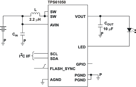
Typical Application Schematic

3 Description
The TPS6105x device is based on a high-frequency synchronous-boost topology with constant current sink to drive single white LEDs. The device uses an inductive fixed-frequency PWM control scheme using small external components, minimizing input ripple current.
The 2-MHz switching frequency allows the use of small and low profile 2.2-μH inductors. To optimize overall efficiency, the device operates with only a 250-mV LED feedback voltage.
The TPS6105x device not only operates as a regulated current source, but also as a standard voltage-boost regulator. This additional operating mode can be useful to supply other high-power devices in the system, such as a hands-free audio power amplifier, or any other component requiring a supply voltage higher than the battery voltage (refer to TPS61052).
For highest flexibility, the LED current or the desired output voltage can be programmed through an I2C compatible interface. To simplify flash synchronization with the camera module, the device offers a trigger pin (FLASH_SYNC) for fast LED turnon time.
When the TPS6105x is not in use, it can be put into shutdown mode through the I2C-compatible interface, reducing the input current to 0.3 μA (typical). During shutdown, the LED pin is high impedance to avoid leakage current through the LED.
Device Information(1)
| PART NUMBER | PACKAGE | BODY SIZE (NOM) |
|---|---|---|
| TPS61050 TPS61052 |
VSON (10) | 3.00 mm × 3.00 mm |
| DSBGA (12) | 1.96 mm × 1.46 mm |
- For all available packages, see the orderable addendum at the end of the data sheet.