JAJSL22F June 2015 – September 2021 TPS61098 , TPS610981 , TPS610982 , TPS610985 , TPS610986 , TPS610987
PRODUCTION DATA
- 1 特長
- 2 アプリケーション
- 3 概要
- 4 Revision History
- 5 Device Comparison Table
- 6 Pin Configuration and Functions
- 7 Specifications
- 8 Detailed Description
- 9 Applications and Implementation
- 10Power Supply Recommendations
- 11Layout
- 12Device and Documentation Support
- 13Mechanical, Packaging, and Orderable Information
8.3.1 Boost Controller Operation
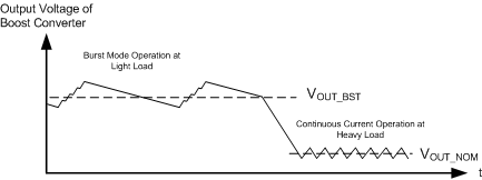
The TPS61098x boost converter is controlled by a hysteretic current mode controller. This controller regulates the output voltage by keeping the inductor ripple current constant in the range of 100 mA and adjusting the offset of this inductor current depending on the output load. Since the input voltage, output voltage and inductor value all affect the rising and falling slopes of inductor ripple current, the switching frequency is not fixed and is decided by the operation condition. If the required average input current is lower than the average inductor current defined by this constant ripple, the inductor current goes discontinuous to keep the efficiency high under light load conditions. Figure 8-1 illustrates the hysteretic current operation. If the load is reduced further, the boost converter enters into Burst mode. In Burst mode, the boost converter ramps up the output voltage with several pulses and it stops operating once the output voltage exceeds a set threshold, and then it goes into a sleep status and consumes less quiescent current. It resumes switching when the output voltage is below the set threshold. It exits the Burst mode when the output current can no longer be supported in this mode. Refer to Figure 8-2 for Burst mode operation details.
To achieve high efficiency, the power stage is realized as a synchronous boost topology. The output voltage V(MAIN) is monitored via an internal feedback network which is connected to the voltage error amplifier. To regulate the output voltage, the voltage error amplifier compares this feedback voltage to the internal voltage reference and adjusts the required offset of the inductor current accordingly.
 Figure 8-1 Hysteretic Current Operation
 Figure 8-2 Burst Mode Operation