SLVSA18A September 2009 – July 2015 TPS61161-Q1
PRODUCTION DATA.
- 1 Features
- 2 Applications
- 3 Description
- 4 Revision History
- 5 Pin Configuration and Functions
- 6 Specifications
- 7 Detailed Description
- 8 Applications and Implementation
- 9 Power Supply Recommendations
- 10Layout
- 11Device and Documentation Support
- 12Mechanical, Packaging, and Orderable Information
パッケージ・オプション
メカニカル・データ(パッケージ|ピン)
- DRV|6
サーマルパッド・メカニカル・データ
- DRV|6
発注情報
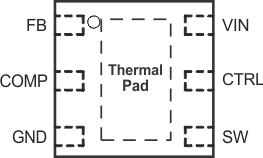
5 Pin Configuration and Functions
DRV Package
6-Pin SON With Thermal Pad
Top View

Pin Functions
| PIN | I/O | DESCRIPTION | |
|---|---|---|---|
| NAME | NO. | ||
| COMP | 2 | O | Output of the transconductance error amplifier. Connect an external capacitor to this pin to compensate the regulator. |
| CTRL | 5 | I | Control pin of the boost regulator. It is a multi-functional pin which can be used for enable control, PWM and digital dimming. |
| FB | 1 | I | Feedback pin for current. Connect the sense resistor from FB to GND. |
| GND | 3 | O | Ground |
| SW | 4 | I | This is the switching node of the IC. Connect the inductor between the VIN and SW pin. This pin is also used to sense the output voltage for open LED protection |
| VIN | 6 | I | The input supply pin for the IC. Connect VIN to a supply voltage from 2.7 V to 18 V. |
| Thermal Pad | — | The thermal pad should be soldered to the analog ground plane. If possible, use thermal via to connect to ground plane for ideal power dissipation. | |