JAJSVH7A October 2024 – November 2024 TPS61287
PRODUCTION DATA
- 1
- 1 特長
- 2 アプリケーション
- 3 概要
- 4 Pin Configuration and Functions
- 5 Specifications
-
6 Detailed Description
- 6.1 Overview
- 6.2 Functional Block Diagram
- 6.3 Feature Description
- 7 Application and Implementation
- 8 Device and Documentation Support
- 9 Revision History
- 10Mechanical, Packaging, and Orderable Information
6.3.3 Programmable EN/UVLO
The TPS61287 has a dual function enable and undervoltage lockout (UVLO) circuit at EN/UVLO pin. When the voltage at the VIN and VCC pin is above the rising threshold of UVLO and the EN/UVLO pin is pulled above 1.18V but below the enable EN/UVLO threshold of 1.23V, the TPS61287 is enabled but still in standby mode.
The EN/UVLO pin has an accurate UVLO voltage threshold to support programmable input undervoltage lockout with hysteresis. When the EN/UVLO pin voltage is greater than the UVLO threshold of 1.23V, the TPS61287 is enabled for switching operation. A hysteresis current, IUVLO_HYS, is sourced out of the EN/UVLO pin to provide a hysteresis that prevents on/off chatter in the presence of noise with a slowly changing input voltage.
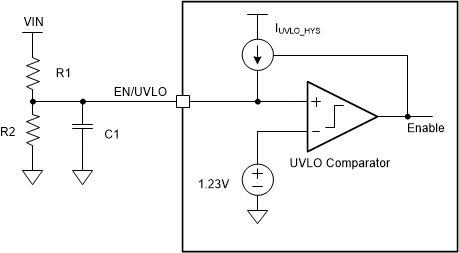
By using resistor divider as shown in Figure 6-1, the turn-on threshold is calculated using Equation 1.

where
- VUVLO is the UVLO threshold of 1.23V at the EN/UVLO pin.
The hysteresis between the UVLO turn-on threshold and turn-off threshold is set by the upper resistor in the EN/UVLO resistor divider and is given by Equation 2.

where
- IUVLO_HYS is the sourcing current from the EN/UVLO pin when the voltage at the EN/UVLO pin is above VUVLO.
 Figure 6-1 Programmable UVLO With
Resistor Divider at the EN/UVLO Pin
Figure 6-1 Programmable UVLO With
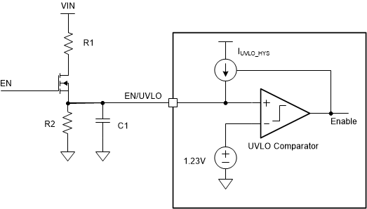
Resistor Divider at the EN/UVLO PinBy using an NMOSFET together with a resistor divider the user can implement both logic enable and programmable UVLO as shown in Figure 6-2. The EN logic high level must be greater than the enable threshold plus the Vth of the NMOSFET Q1. The Q1 also eliminates the leakage current from VIN to ground through the UVLO resistor divider during shutdown mode.
 Figure 6-2 Logic Enable and Programmable
UVLO