JAJSFB0E January 2018 – February 2024 TPS61322
PRODUCTION DATA
- 1
- 1 特長
- 2 アプリケーション
- 3 概要
- 4 Device Comparison Table
- 5 Pin Configuration and Functions
- 6 Specifications
- 7 Detailed Description
- 8 Application and Implementation
- 9 Power Supply Recommendations
- 10Layout
- 11Device and Documentation Support
- 12Revision History
- 13Mechanical, Packaging, and Orderable Information
パッケージ・オプション
メカニカル・データ(パッケージ|ピン)
サーマルパッド・メカニカル・データ
発注情報
8.2.1.2.3 Inductor Selection
Because the inductor affects steady state operation, transient behavior, and loop stability, the inductor is the most important component in power regulator design. There are three important inductor specifications, inductor value, saturation current, and dc resistance (DCR).
The TPS61322xx is optimized to work with inductor values between 0.7 µH and 13 µH. The inductor values affect the switching frequency. The estimated switching frequency in continuous conduction mode(CCM) can be calculated by Equation 2. The switching frequency ƒSW is not a constant value, which is determined by the inductance, the inductor current ripple, the input voltage and the output voltage. The current ripple ILH is fixed to 200 mA typically, but it can be affected by the inductor value indirectly. Normally when a smaller inductor value is applied, the inductor current ramps up and down more quickly. The current ripple becomes bigger because the internal current comparator has delay to respond. If a smaller inductor peak current is required in applications, a higher inductor value can be used. However, The inductor and output capacitor must be considered together for the loop stability. The output capacitor and the inductance will influence the bandwidth and phase margin of the converter. Consequently, with a larger inductor, a bigger capacitor normally must be used to ensure the same L/C ratio for a stable loop. For best stability consideration, a 4.7-µH inductor is recommended for 2.2-V output voltage application.

where
- fSW is the switching frequency of the converter
- ILH is the inductor current ripple
- η is the boost converter power convert efficiency
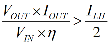
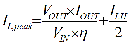
Having selected the inductance value, follow Equation 3 to Equation 5 to calculate the inductor's peak current for the application. Depending on different load conditions, the TPS61322xx works in continuous current mode or discontinuous conduction mode(DCM). In different modes, the peak currents of the inductor are also different. Equation 3 provides an easy way to estimate whether the device works in CCM or DCM. Equation 4 shows the peak current when the device works in CCM and Equation 5 shows the peak current when the device works in DCM.

where
- ILH is the inductor current ripple
- η is the boost converter power convert efficiency

where
- IL,peak is the peak current of the inductor
- ILH is the inductor current ripple
- η is the boost converter power convert efficiency

where
- IL,peak is the peak inductor.
- ILH is the inductor current ripple
The saturation current of the inductor must be higher than the calculated peak inductor current, otherwise the excessive peak current in the inductor harms the device and reduces the system reliability.