JAJSI60 November 2019 TPS61391
PRODUCTION DATA.
- 1 特長
- 2 アプリケーション
- 3 概要
- 4 改訂履歴
- 5 Pin Configuration and Functions
- 6 Specifications
- 7 Detailed Description
-
8 Application and Implementation
- 8.1 Application Information
- 8.2
Typical Application
- 8.2.1 Design Requirement
- 8.2.2
Detailed Design Procedure
- 8.2.2.1 Selecting the Rectifier Diode
- 8.2.2.2 Selecting the Inductor
- 8.2.2.3 Selecting Output Capacitor
- 8.2.2.4 Selecting Filter Resistor and Capacitor
- 8.2.2.5 Setting the Output Voltage
- 8.2.2.6 Selecting Capacitor for CAP pin
- 8.2.2.7 Selecting Capacitor for AVCC pin
- 8.2.2.8 Selecting Capacitor for APD pin
- 8.2.2.9 Selecting the Resistors of MON1 or MON2
- 8.2.2.10 Selecting the Capacitors of MON1 or MON2
- 8.2.2.11 Selecting the Short Current Limit
- 8.2.3 Application Curves
- 9 Power Supply Recommendations
- 10Layout
- 11デバイスおよびドキュメントのサポート
- 12メカニカル、パッケージ、および注文情報
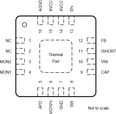
5 Pin Configuration and Functions
RTE Package
16-Pin WQFN
Top View

Pin Functions
| PIN | I/O | DESCRIPTION | ||
|---|---|---|---|---|
| NAME | NO. | |||
| NC | 1,2 | N/A | No internal connection | |
| MON2 | 3 | O | Current mirror output pin of 1 : 5 ratio (Mirror current: APD current) | |
| MON1 | 4 | O | Current mirror output pin of 4 : 5 ratio (Mirror current: APD current) | |
| APD | 5 | O | Power supply for the APD, connect this pin with the cathode of APD | |
| MONIN | 6 | I | Current mirror input pin | |
| GND | 7 | – | Power Ground | |
| SW | 8 | PWR | The switching node pin of the converter. It is connected to the drain of the internal low-side power MOSFET and the source of the internal high-side power MOSFET | |
| CAP | 9 | O | Connecting a capacitor externally to lower the noise for current mirror. | |
| VIN | 10 | I | IC power supply input | |
| ISHORT | 11 | O | Programming the current limit for high optical power protection by a resistor between this pin and GND. | |
| FB | 12 | I | Feedback voltage | |
| EN | 13 | I | Enable logic input. Logic high level enables the device. Logic low level disables the device and turns it into shutdown mode | |
| AVCC | 14,15 | I | Power supply for the current monitor circuitry | |
| AGND | 16 | – | Analog ground for the current monitor circuitry | |
| Exposed Thermal Pad | Connect with GND, TI recommends connecting to Power GND on PCB | |||