JAJS521F December 2008 – May 2019 TPS61500
PRODUCTION DATA.
- 1 特長
- 2 アプリケーション
- 3 概要
- 4 改訂履歴
- 5 Pin Configuration and Functions
- 6 Specifications
- 7 Detailed Description
-
8 Application and Implementation
- 8.1 Application Information
- 8.2
Typical Applications
- 8.2.1
Analog Dimming Method
- 8.2.1.1 Design Requirements
- 8.2.1.2
Detailed Design Procedure
- 8.2.1.2.1 Programming the Overvoltage Protection
- 8.2.1.2.2 Programming the LED Current
- 8.2.1.2.3 Implementing Dimming
- 8.2.1.2.4 Computing the Maximum Output Current
- 8.2.1.2.5 Selecting the Inductor
- 8.2.1.2.6 Selecting the Schottky Diode
- 8.2.1.2.7 Selecting the Compensation Capacitor and Resistor
- 8.2.1.2.8 Selecting the Input and Output Capacitor
- 8.2.1.3 Application Curves
- 8.2.2 Pure PWM Dimming Method
- 8.2.1
Analog Dimming Method
- 9 Power Supply Recommendations
- 10Layout
- 11デバイスおよびドキュメントのサポート
- 12メカニカル、パッケージ、および注文情報
パッケージ・オプション
メカニカル・データ(パッケージ|ピン)
- PWP|14
サーマルパッド・メカニカル・データ
- PWP|14
発注情報
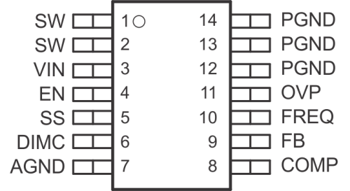
5 Pin Configuration and Functions
PWP Package
14-Pin HTSSOP With Thermal Pad
Top View

Pin Functions
| PIN | I/O | DESCRIPTION | |
|---|---|---|---|
| NAME | NO. | ||
| AGND | 7 | I | Signal ground of the IC |
| COMP | 8 | O | Output of the transconductance error amplifier. An external RC network is connected to this pin. |
| DIMC | 6 | I | Analog and PWM dimming method option pin. A capacitor connected to the pin to set the time constant of reference for analog dimming. Float this pin for PWM dimming. |
| EN | 4 | I | Enable pin. When the voltage of this pin falls below the enable threshold for more than 10 ms, the IC turns off. This pin is also used for PWM signal input for LED brightness dimming. |
| FB | 9 | I | Feedback pin for positive voltage regulation. A resistor connects to this pin to program LED current. |
| FREQ | 10 | O | Switch frequency program pin. An external resistor is connected to this pin. See Application Information for information on how to size the FREQ resistor. |
| OVP | 11 | I | Overvoltage protection for LED driver. The voltage is 1.229 V. Using a resistor divider can program the threshold of OVP. |
| PGND | 12-14 | I | Power ground of the IC. It is connected to the source of the PWM switch. |
| SS | 5 | O | Soft start programming pin. A capacitor between the SS pin and GND pin programs soft-start timing. See Application and Implementation for information on how to size the SS capacitor |
| SW | 1, 2 | I | This is the switching node of the IC. Connect SW to the switched side of the inductor. |
| Thermal Pad | — | — | Solder the thermal pad to the analog ground. If possible, use thermal via to connect to top and internal ground plane layers for ideal power dissipation. |
| VIN | 3 | I | The input pin to the IC. Connect VIN to a supply voltage between 2.9 V and 18 V. It is acceptable for the voltage on the pin to be different from the boost power stage input for applications requiring voltage beyond VIN range. |