JAJSJ58B january 2015 – august 2023 TPS62065-Q1 , TPS62067-Q1
PRODUCTION DATA
- 1
- 1 特長
- 2 アプリケーション
- 3 概要
- 4 Revision History
- 5 Device Comparison Table
- 6 Pin Configuration and Functions
- 7 Specifications
- 8 Parameter Measurement Information
-
9 Detailed Description
- 9.1 Overview
- 9.2 Functional Block Diagram
- 9.3
Feature Description
- 9.3.1 Mode Selection (TPS62065-Q1) and Forced PWM Mode (TPS62067A-Q1)
- 9.3.2 Power Good (PG, TPS62067x-Q1)
- 9.3.3 Enable
- 9.3.4 Shutdown and Output Discharge
- 9.3.5 Soft Start
- 9.3.6 Undervoltage Lockout (UVLO)
- 9.3.7 Internal Current Limit and Foldback Current Limit For Short-Circuit Protection
- 9.3.8 Clock Dithering
- 9.3.9 Thermal Shutdown
- 9.4 Device Functional Modes
- 10Application and Implementation
- 11Device and Documentation Support
- 12Mechanical, Packaging, and Orderable Information
パッケージ・オプション
メカニカル・データ(パッケージ|ピン)
- DSG|8
サーマルパッド・メカニカル・データ
- DSG|8
発注情報
10.2.3 Application Curves
Table 10-3 Table of Graphs
| FIGURE | |||
|---|---|---|---|
| η | Efficiency | Load Current, VOUT = 1.2 V, Auto PFM and PWM Mode, Linear Scale | Figure 10-3 |
| Load Current, VOUT = 1.8 V, Auto PFM and PWM Mode, Linear Scale | Figure 10-4 | ||
| Load Current, VOUT = 3.3 V, PFM and PWM Mode, Linear Scale | Figure 10-5 | ||
| Load Current, VOUT = 1.8 V, Auto PFM and PWM Mode vs. Forced PWM Mode, Logarithmic Scale | Figure 10-6 | ||
| Output Voltage Accuracy | Load Current, VOUT = 1.8 V, Auto PFM and PWM Mode | Figure 10-7 | |
| Load Current, VOUT = 1.8 V, Forced PWM Mode | Figure 10-8 | ||
| Typical Operation | PWM Mode, VIN = 3.6 V, VOUT = 1.8 V, 500 mA, L = 1.2 μH, COUT = 10 μF | Figure 10-9 | |
| PFM Mode, VIN = 3.6 V, VOUT = 1.8 V, 20 mA, L = 1.2 μH, COUT = 10 μF | Figure 10-10 | ||
| Load Transient | PWM Mode, VIN = 3.6 V, VOUT = 1.2 V, 0.2 mA to 1 A | Figure 10-11 | |
| PFM Mode, VIN = 3.6 V, VOUT = 1.2 V, 20 mA to 250 mA | Figure 10-12 | ||
| VIN = 3.6 V, VOUT = 1.8 V, 200 mA to 1500 mA | Figure 10-13 | ||
| Line Transient | PWM Mode, VIN = 3.6 V to 4.2 V, VOUT = 1.8 V, 500 mA | Figure 10-14 | |
| PFM Mode, VIN = 3.6 V to 4.2 V, VOUT = 1.8 V, 500 mA | Figure 10-15 | ||
| Start-Up into Load | VIN = 3.6 V, VOUT = 1.8 V, Load = 2.2 Ω | Figure 10-16 | |
| Start-Up TPS62067-Q1 | Into 2.2-Ω Load with Power Good | Figure 10-17 | |
| Output Discharge | VIN = 3.6 V, VOUT = 1.8 V, No Load | Figure 10-18 | |
| Shutdown TPS62067-Q1 | VIN = 4.2 V, VOUT = 3.3 V, No Load, PG Pullup Resistor 10 kΩ | Figure 10-19 | |
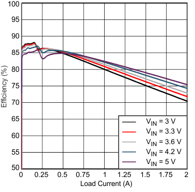
| VOUT = 1.2 V | Linear Scale | |
| L = 1.2 µH (NRG4026T 1R2) | COUT = 10 µF (0603 size) | |
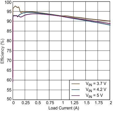
| VOUT = 3.3 V | Linear Scale | |
| L = 1.2 µH (NRG4026T 1R2) | COUT = 22 µF (0603 size) | |

| L = 1 µH | VOUT = 1.8 V | COUT = 10 µF |
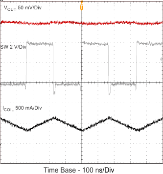
| VIN = 3.6 V | VOUT = 1.8 V | MODE = GND |
| COUT = 10 µF | L = 1.2 µH | IOUT = 500 mA |
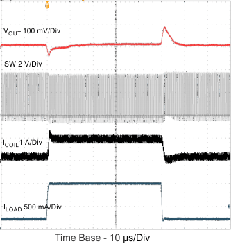
| VIN = 3.6 V | VOUT = 1.2 V | IOUT = 0.2 to 1 A |
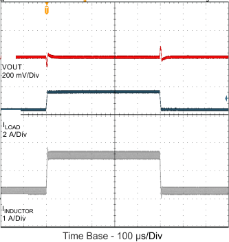
| VIN = 3.6 V | VOUT = 1.8 V | L = 1.2 µH |
| COUT = 10 µF | ||
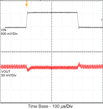
| VIN = 3.6 to 4.2 V | VOUT = 1.8 V | IOUT = 50 mA |
| COUT = 10 µF | L = 1.2 µH |
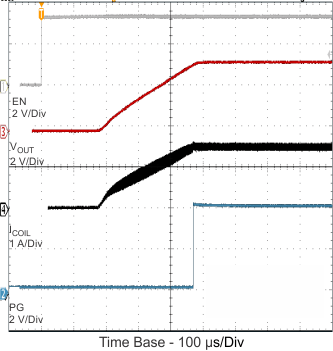
| VIN = 4.2 V | VOUT = 3.3 V | Load = 2R2 |
| PG Pullup resistor 10 kΩ | ||

| VIN = 4.2 V | VOUT = 3.3 V | No load | ||
| PG pullup resistor, 10 kΩ | ||||

| VOUT = 1.8 V | Linear Scale | |
| L = 1.2 µH (NRG4026T 1R2) | COUT = 10 µF (0603 size) | |
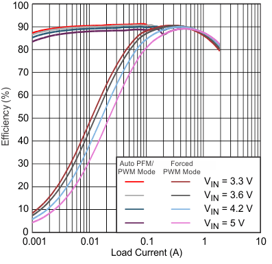
| VOUT = 1.8 V | Logarithmic Scale | |
| COUT = 10 µF (0603 size) | L = 1.2 µH (NRG4026T 1R2) | |
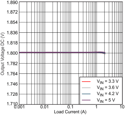
| L = 1 µH | VOUT = 1.8 V | COUT = 10 µF |

| VIN = 3.6 V | VOUT = 1.8 V | MODE = GND |
| COUT = 10 µF | L = 1.2 µH | IOUT = 20 mA |

| VIN = 3.6 V | VOUT = 1.8 V | IOUT = 20 to 750 mA |
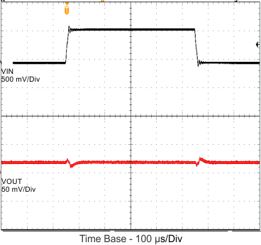
| VIN = 3.6 to 4.2 V | VOUT = 1.8 V | IOUT = 500 mA |
| COUT = 10 µF | L = 1.2 µH |

| VIN = 3.6 V | VOUT = 1.8 V | Load = 2R2 |
| COUT = 10 µF | L = 1.2 µH |

| VIN = 3.6 V | VOUT = 1.8 V | No load |
| COUT = 1.8 µF |