JAJSJ58B january 2015 – august 2023 TPS62065-Q1 , TPS62067-Q1
PRODUCTION DATA
- 1
- 1 特長
- 2 アプリケーション
- 3 概要
- 4 Revision History
- 5 Device Comparison Table
- 6 Pin Configuration and Functions
- 7 Specifications
- 8 Parameter Measurement Information
-
9 Detailed Description
- 9.1 Overview
- 9.2 Functional Block Diagram
- 9.3
Feature Description
- 9.3.1 Mode Selection (TPS62065-Q1) and Forced PWM Mode (TPS62067A-Q1)
- 9.3.2 Power Good (PG, TPS62067x-Q1)
- 9.3.3 Enable
- 9.3.4 Shutdown and Output Discharge
- 9.3.5 Soft Start
- 9.3.6 Undervoltage Lockout (UVLO)
- 9.3.7 Internal Current Limit and Foldback Current Limit For Short-Circuit Protection
- 9.3.8 Clock Dithering
- 9.3.9 Thermal Shutdown
- 9.4 Device Functional Modes
- 10Application and Implementation
- 11Device and Documentation Support
- 12Mechanical, Packaging, and Orderable Information
パッケージ・オプション
メカニカル・データ(パッケージ|ピン)
- DSG|8
サーマルパッド・メカニカル・データ
- DSG|8
発注情報
10.2.2.2.1 Inductor Selection
The inductor value has a direct effect on the ripple current. The selected inductor has to be rated for its DC resistance and saturation current. The inductor ripple current (ΔIL) decreases with higher inductance and increases with higher VI or VO.
Equation 6 calculates the maximum inductor current in PWM mode under static load conditions. The saturation current of the inductor must be rated higher than the maximum inductor current as calculated with Equation 7. TI makes this recommendation because during heavy load transient, the inductor current rises above the calculated value.
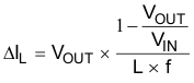
where
- ΔIL = peak-to-peak inductor ripple current
- L = inductor value
- f = switching frequency (3-MHz typical)
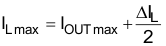
where
- ILmax = maximum inductor current
A more conservative approach is to select the inductor current rating just for the switch current limit ILIMF of the converter.
The total losses of the coil have a strong impact on the efficiency of the DC/DC conversion and consist of both the losses in the DC resistance R(DC) and the following frequency-dependent components:
- The losses in the core material (magnetic hysteresis loss, especially at high switching frequencies)
- Additional losses in the conductor from the skin effect (current displacement at high frequencies)
- Magnetic field losses of the neighboring windings (proximity effect)
| INDUCTOR TYPE | INDUCTANCE (μH) | CURRENT (A) | DIMENSIONS (mm) | MANUFACTURER |
|---|---|---|---|---|
| XEL4020-102ME | 1.0 | 13.25 | 4 × 4 × 2 | Coilcraft |
| DFE252012PD-1R0M | 1.0 | 3.8 | 2.5 × 2.0 × 1.2 | Murata |