JAJSEC9D May 2014 – January 2018 TPS6213013A-Q1 , TPS62130A-Q1 , TPS62133A-Q1
PRODUCTION DATA.
- 1 特長
- 2 アプリケーション
- 3 概要
- 4 改訂履歴
- 5 Device Comparison Table
- 6 Pin Configuration and Functions
- 7 Specifications
- 8 Parameter Measurement Information
-
9 Detailed Description
- 9.1 Overview
- 9.2 Functional Block Diagram
- 9.3
Feature Description
- 9.3.1 Pulse Width Modulation (PWM) Operation
- 9.3.2 Power Save Mode Operation
- 9.3.3 100% Duty-Cycle Operation
- 9.3.4 Enable / Shutdown (EN)
- 9.3.5 Soft Start / Tracking (SS/TR)
- 9.3.6 Current Limit And Short Circuit Protection
- 9.3.7 Power Good (PG)
- 9.3.8 Pin-Selectable Output Voltage (DEF)
- 9.3.9 Frequency Selection (FSW)
- 9.3.10 Under Voltage Lockout (UVLO)
- 9.3.11 Thermal Shutdown
- 9.4 Device Functional Modes
-
10Application and Implementation
- 10.1 Application Information
- 10.2
Typical Application
- 10.2.1
TPS62130A-Q1 Point-Of-Load Step Down Converter
- 10.2.1.1 Design Requirements
- 10.2.1.2
Detailed Design Procedure
- 10.2.1.2.1 Custom Design With WEBENCH® Tools
- 10.2.1.2.2 Programming The Output Voltage
- 10.2.1.2.3 External Component Selection
- 10.2.1.2.4 Inductor Selection
- 10.2.1.2.5 Output Capacitor
- 10.2.1.2.6 Input Capacitor
- 10.2.1.2.7 Soft Start Capacitor
- 10.2.1.2.8 Tracking Function
- 10.2.1.2.9 Output Filter And Loop Stability
- 10.2.1.3 Application Curves
- 10.2.1
TPS62130A-Q1 Point-Of-Load Step Down Converter
- 10.3 System Examples
- 11Power Supply Recommendations
- 12Layout
- 13デバイスおよびドキュメントのサポート
- 14メカニカル、パッケージ、および注文情報
パッケージ・オプション
デバイスごとのパッケージ図は、PDF版データシートをご参照ください。
メカニカル・データ(パッケージ|ピン)
- RGT|16
サーマルパッド・メカニカル・データ
発注情報
10.2.1.2.8 Tracking Function
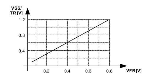
If a tracking function is desired, the SS/TR pin can be used for this purpose by connecting it to an external tracking voltage. The output voltage tracks that voltage. If the tracking voltage is between 50mV and 1.2V, the FB pin tracks the SS/TR pin voltage as described in Equation 11 and shown in Figure 11.
spacing

 Figure 11. Voltage Tracking Relationship
Once the SS/TR pin voltage reaches about 1.2V, the internal voltage is clamped to the internal feedback voltage and device goes to normal regulation. This works for rising and falling tracking voltages with the same behavior, as long as the input voltage is inside the recommended operating conditions. For decreasing SS/TR pin voltage, the device doesn't sink current from the output. So, the resulting decrease of the output voltage may be slower than the SS/TR pin voltage if the load is light. When driving the SS/TR pin with an external voltage, do not exceed the voltage rating of the SS/TR pin which is VIN+0.3V.
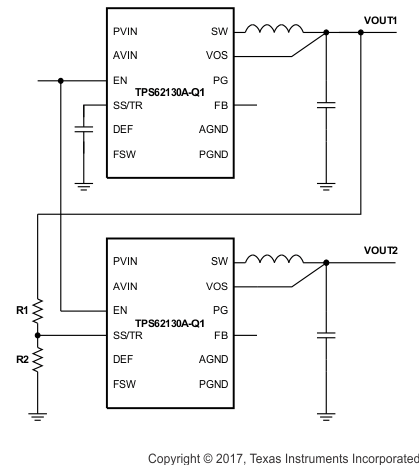
If the input voltage drops into undervoltage lockout or even down to zero, the output voltage will go to zero, independent of the tracking voltage. Figure 12 shows how to connect devices to get ratiometric and simultaneous sequencing by using the tracking function.
spacing
 Figure 12. Sequence for Ratiometric and Simultaneous Startup
 spacing
The resistive divider of R1 and R2 can be used to change the ramp rate of VOUT2 faster, slower or the same as VOUT1.
A sequential startup is achieved by connecting the PG pin of VOUT1 to the EN pin of VOUT2. Ratiometric start up sequence happens if both supplies are sharing the same soft start capacitor. Equation 10 calculates the soft start time, though the SS/TR current has to be doubled. Details about these and other tracking and sequencing circuits are found in SLVA470.
Note: If the voltage at the FB pin is below its typical value of 0.8V, the output voltage accuracy may have a wider tolerance than specified.