JAJSEC9D May   2014  – January 2018 TPS6213013A-Q1 , TPS62130A-Q1 , TPS62133A-Q1

PRODUCTION DATA.  

  1. 特長
  2. アプリケーション
  3. 概要
    1.     Device Images
      1.      代表的なアプリケーションの回路図
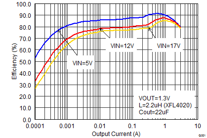
      2.      効率と出力電流との関係
  4. 改訂履歴
  5. Device Comparison Table
  6. Pin Configuration and Functions
    1.     Pin Functions
  7. Specifications
    1. 7.1 Absolute Maximum Ratings
    2. 7.2 ESD Ratings
    3. 7.3 Recommended Operating Conditions
    4. 7.4 Thermal Information
    5. 7.5 Electrical Characteristics
    6. 7.6 Typical Characteristics
  8. Parameter Measurement Information
  9. Detailed Description
    1. 9.1 Overview
    2. 9.2 Functional Block Diagram
    3. 9.3 Feature Description
      1. 9.3.1  Pulse Width Modulation (PWM) Operation
      2. 9.3.2  Power Save Mode Operation
      3. 9.3.3  100% Duty-Cycle Operation
      4. 9.3.4  Enable / Shutdown (EN)
      5. 9.3.5  Soft Start / Tracking (SS/TR)
      6. 9.3.6  Current Limit And Short Circuit Protection
      7. 9.3.7  Power Good (PG)
      8. 9.3.8  Pin-Selectable Output Voltage (DEF)
      9. 9.3.9  Frequency Selection (FSW)
      10. 9.3.10 Under Voltage Lockout (UVLO)
      11. 9.3.11 Thermal Shutdown
    4. 9.4 Device Functional Modes
      1. 9.4.1 Operation Above TJ=125°C
      2. 9.4.2 Operation with VIN < 3V
      3. 9.4.3 Operation with Separate EN Control
  10. 10Application and Implementation
    1. 10.1 Application Information
    2. 10.2 Typical Application
      1. 10.2.1 TPS62130A-Q1 Point-Of-Load Step Down Converter
        1. 10.2.1.1 Design Requirements
        2. 10.2.1.2 Detailed Design Procedure
          1. 10.2.1.2.1 Custom Design With WEBENCH® Tools
          2. 10.2.1.2.2 Programming The Output Voltage
          3. 10.2.1.2.3 External Component Selection
          4. 10.2.1.2.4 Inductor Selection
          5. 10.2.1.2.5 Output Capacitor
          6. 10.2.1.2.6 Input Capacitor
          7. 10.2.1.2.7 Soft Start Capacitor
          8. 10.2.1.2.8 Tracking Function
          9. 10.2.1.2.9 Output Filter And Loop Stability
        3. 10.2.1.3 Application Curves
    3. 10.3 System Examples
      1. 10.3.1 Regulated Power LED Supply
      2. 10.3.2 Inverting Power Supply
      3. 10.3.3 Active Output Discharge
      4. 10.3.4 Various Output Voltages
  11. 11Power Supply Recommendations
  12. 12Layout
    1. 12.1 Layout Guidelines
    2. 12.2 Layout Example
  13. 13デバイスおよびドキュメントのサポート
    1. 13.1 デバイス・サポート
      1. 13.1.1 デベロッパー・ネットワークの製品に関する免責事項
    2. 13.2 関連リンク
    3. 13.3 ドキュメントの更新通知を受け取る方法
    4. 13.4 コミュニティ・リソース
    5. 13.5 商標
    6. 13.6 静電気放電に関する注意事項
    7. 13.7 Glossary
  14. 14メカニカル、パッケージ、および注文情報

パッケージ・オプション

デバイスごとのパッケージ図は、PDF版データシートをご参照ください。

メカニカル・データ(パッケージ|ピン)
  • RGT|16
サーマルパッド・メカニカル・データ
発注情報

Application Curves

At VIN=12V, VOUT=3.3V and TA=25°C, FSW=Low, (unless otherwise noted)
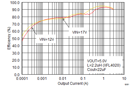
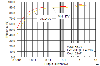
TPS62130A-Q1 TPS62133A-Q1 TPS6213013A-Q1 SLVSCC2_eff50iout.png
FSW = Low
Figure 13. Efficiency vs. Output Current
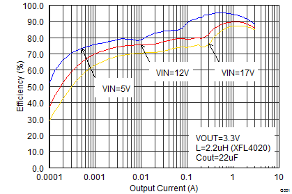
TPS62130A-Q1 TPS62133A-Q1 TPS6213013A-Q1 SLVSCC2_eff50iouthalf.png
FSW = High
Figure 15. Efficiency vs. Output Current
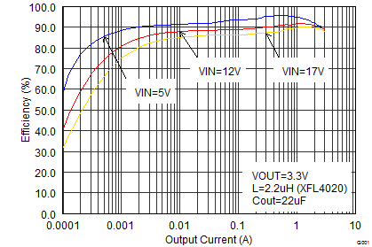
TPS62130A-Q1 TPS62133A-Q1 TPS6213013A-Q1 SLVSCC2_eff33iout.png
FSW = Low
Figure 17. Efficiency vs. Output Current
TPS62130A-Q1 TPS62133A-Q1 TPS6213013A-Q1 SLVSCC2_eff33iouthalf.png
FSW = High
Figure 19. Efficiency vs. Output Current
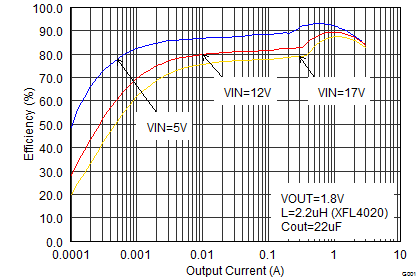
TPS62130A-Q1 TPS62133A-Q1 TPS6213013A-Q1 SLVSCC2_eff18iouthalf.png
FSW = High
Figure 21. Efficiency vs. Output Current
TPS62130A-Q1 TPS62133A-Q1 TPS6213013A-Q1 SLVSCC2_eff13iouthalf.gif
FSW = High
Figure 23. Efficiency vs. Output Current
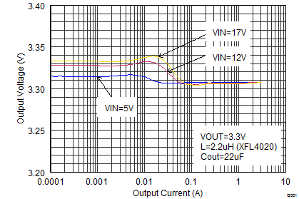
TPS62130A-Q1 TPS62133A-Q1 TPS6213013A-Q1 SLVSCC2_loadreg.png
L = 2.2 µH (XFL4020) COUT = 22 µH
Figure 25. Output Voltage Accuracy (Load Regulation)
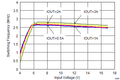
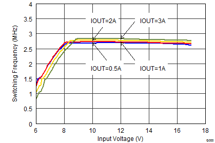
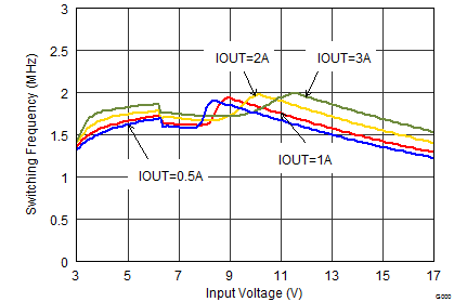
TPS62130A-Q1 TPS62133A-Q1 TPS6213013A-Q1 SLVSCC2_fswvin_5.0V.png
VOUT = 5 V L = 2.2 µH (XFL4020) COUT = 22 µH
Figure 27. Switching Frequency vs. Input Voltage
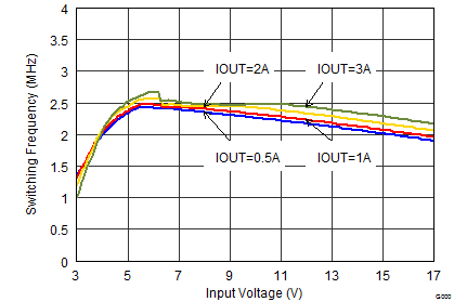
TPS62130A-Q1 TPS62133A-Q1 TPS6213013A-Q1 SLVSCC2_fswvin_3.3V.png
VOUT = 3.3 V L = 2.2 µH (XFL4020) COUT = 22 µH
Figure 29. Switching Frequency vs. Input Voltage
TPS62130A-Q1 TPS62133A-Q1 TPS6213013A-Q1 SLVSCC2_fswvin_1.8V.png
VOUT = 1.8 V L = 2.2 µH (XFL4020) COUT = 22 µH
Figure 31. Switching Frequency vs. Input Voltage
TPS62130A-Q1 TPS62133A-Q1 TPS6213013A-Q1 SLVSCC2_fswvin_1.0V.png
VOUT = 1 V L = 2.2 µH (XFL4020) COUT = 22 µH
Figure 33. Switching Frequency vs. Input Voltage
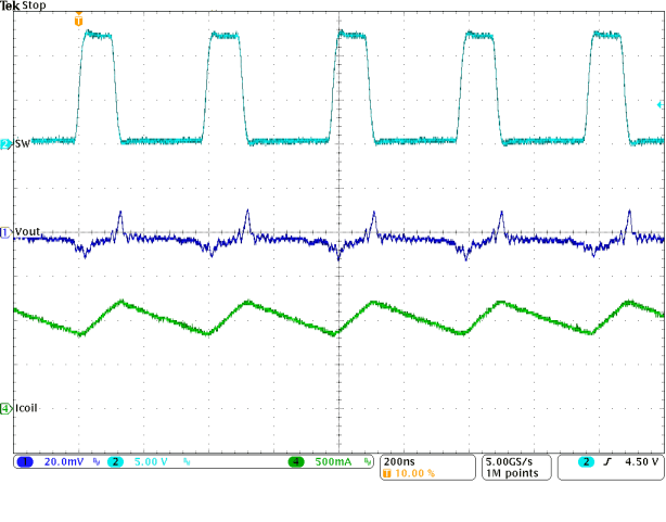
TPS62130A-Q1 TPS62133A-Q1 TPS6213013A-Q1 SLVSCC2_PWMtyp.gifFigure 35. Typical Operation in PWM Mode (IOUT= 1 A)
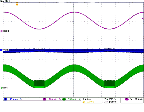
TPS62130A-Q1 TPS62133A-Q1 TPS6213013A-Q1 SLVSCC2_modetran.gifFigure 37. PWM-PSM-Transition
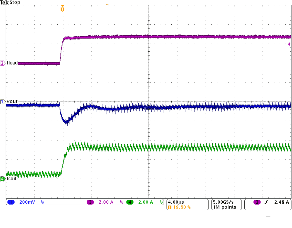
TPS62130A-Q1 TPS62133A-Q1 TPS6213013A-Q1 SLVSCC2_loadtranrise.gifFigure 39. Load Transient Response of Figure 38,
Rising Edge
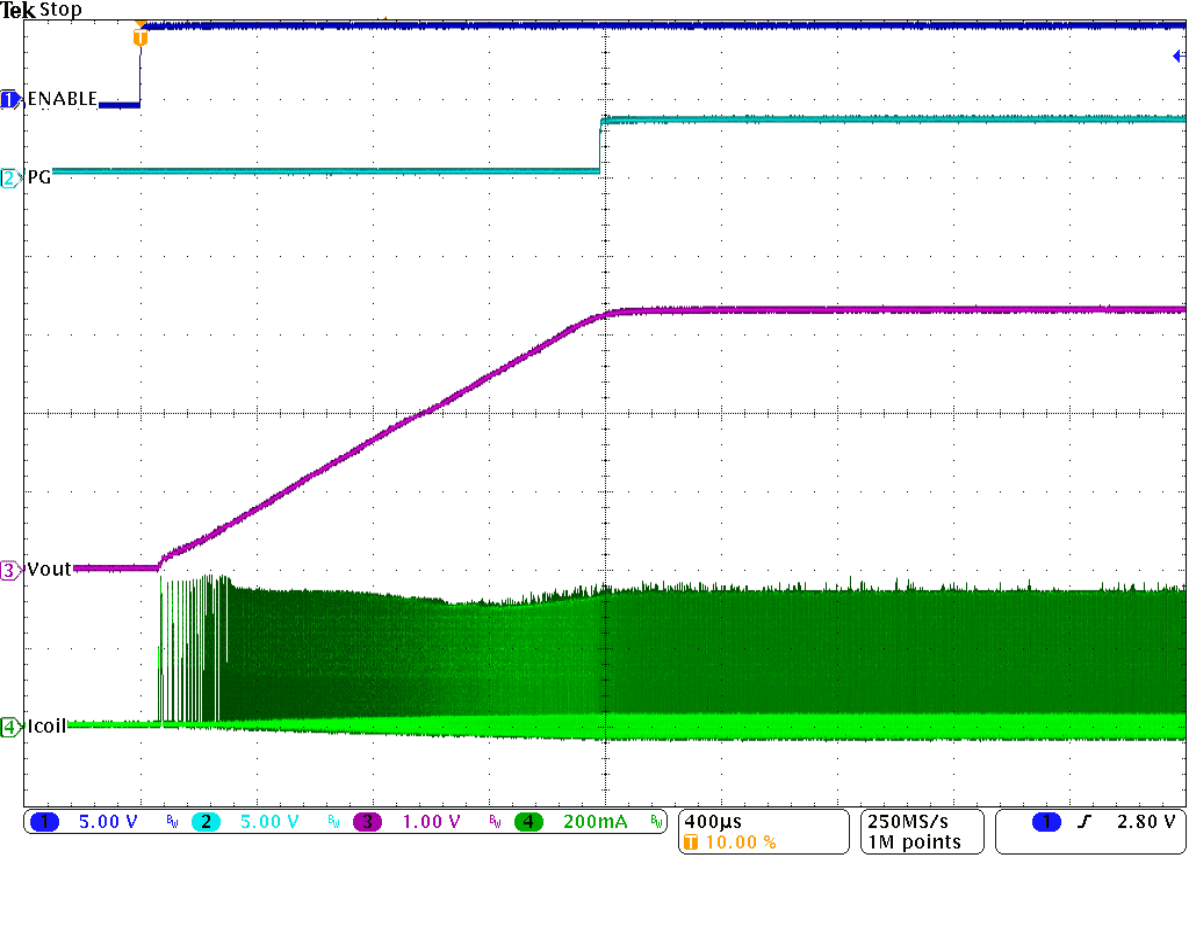
TPS62130A-Q1 TPS62133A-Q1 TPS6213013A-Q1 SLVSCC2_stuplow.gifFigure 41. Start Up into 100 mA
TPS62130A-Q1 TPS62133A-Q1 TPS6213013A-Q1 SLVSCC2_ambienttmp.gif
L = 2.2 µH (XFL4020) TPS62130EVM
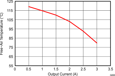
Figure 43. Maximum Ambient Temperature
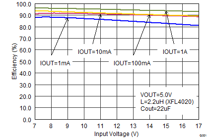
TPS62130A-Q1 TPS62133A-Q1 TPS6213013A-Q1 SLVSCC2_eff50vin.png
FSW = Low
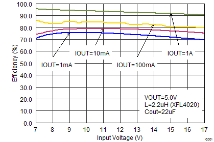
Figure 14. Efficiency vs. Input Voltage
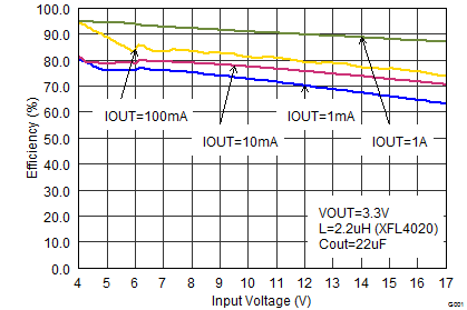
TPS62130A-Q1 TPS62133A-Q1 TPS6213013A-Q1 SLVSCC2_eff50vinhalf.png
FSW = High
Figure 16. Efficiency vs. Input Voltage
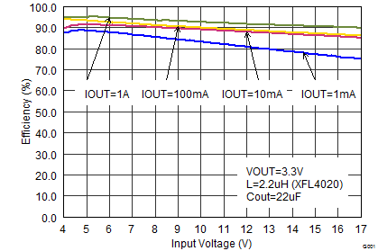
TPS62130A-Q1 TPS62133A-Q1 TPS6213013A-Q1 SLVSCC2_eff33vin.png
FSW = Low
Figure 18. Efficiency vs. Input Voltage
TPS62130A-Q1 TPS62133A-Q1 TPS6213013A-Q1 SLVSCC2_eff33vinhalf.png
FSW = High
Figure 20. Efficiency vs. Input Voltage
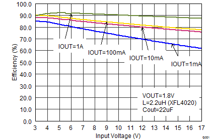
TPS62130A-Q1 TPS62133A-Q1 TPS6213013A-Q1 SLVSCC2_eff18vinhalf.png
FSW = High
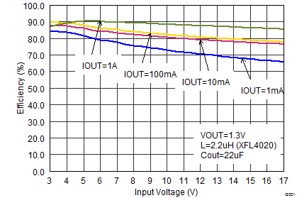
Figure 22. Efficiency vs. Input Voltage
TPS62130A-Q1 TPS62133A-Q1 TPS6213013A-Q1 SLVSCC2_eff13vinhalf.gif
FSW = High
Figure 24. Efficiency vs. Input Voltage
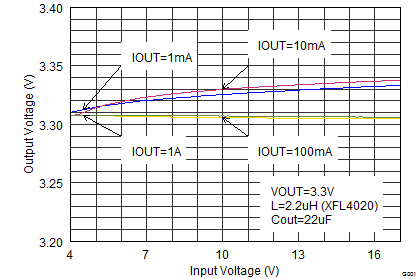
TPS62130A-Q1 TPS62133A-Q1 TPS6213013A-Q1 SLVSCC2_linereg.png
L = 2.2 µH (XFL4020) COUT = 22 µH
Figure 26. Output Voltage Accuracy (Line Regulation)
TPS62130A-Q1 TPS62133A-Q1 TPS6213013A-Q1 SLVSCC2_fswiout_5.0V.png
VOUT = 5 V L = 2.2 µH (XFL4020)
Figure 28. Switching Frequency vs. Output Current
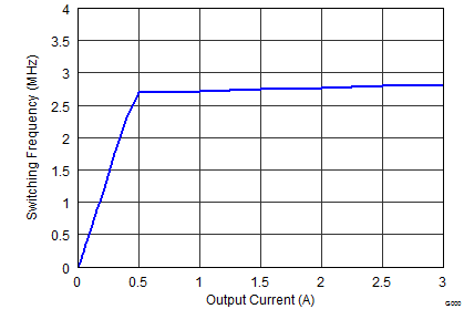
TPS62130A-Q1 TPS62133A-Q1 TPS6213013A-Q1 SLVSCC2_fswiout_3.3V.png
VOUT = 3.3 V L = 2.2 µH (XFL4020)
Figure 30. Switching Frequency vs. Output Current
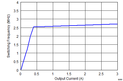
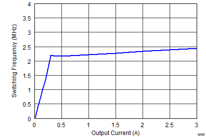
TPS62130A-Q1 TPS62133A-Q1 TPS6213013A-Q1 SLVSCC2_fswiout_1.8V.png
VOUT = 1.8 V L = 2.2 µH (XFL4020)
Figure 32. Switching Frequency vs. Output Current
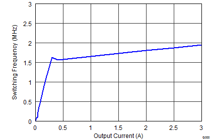
TPS62130A-Q1 TPS62133A-Q1 TPS6213013A-Q1 SLVSCC2_fswiout_1.0V.png
VOUT = 1 V L = 2.2 µH (XFL4020)
Figure 34. Switching Frequency vs. Output Current
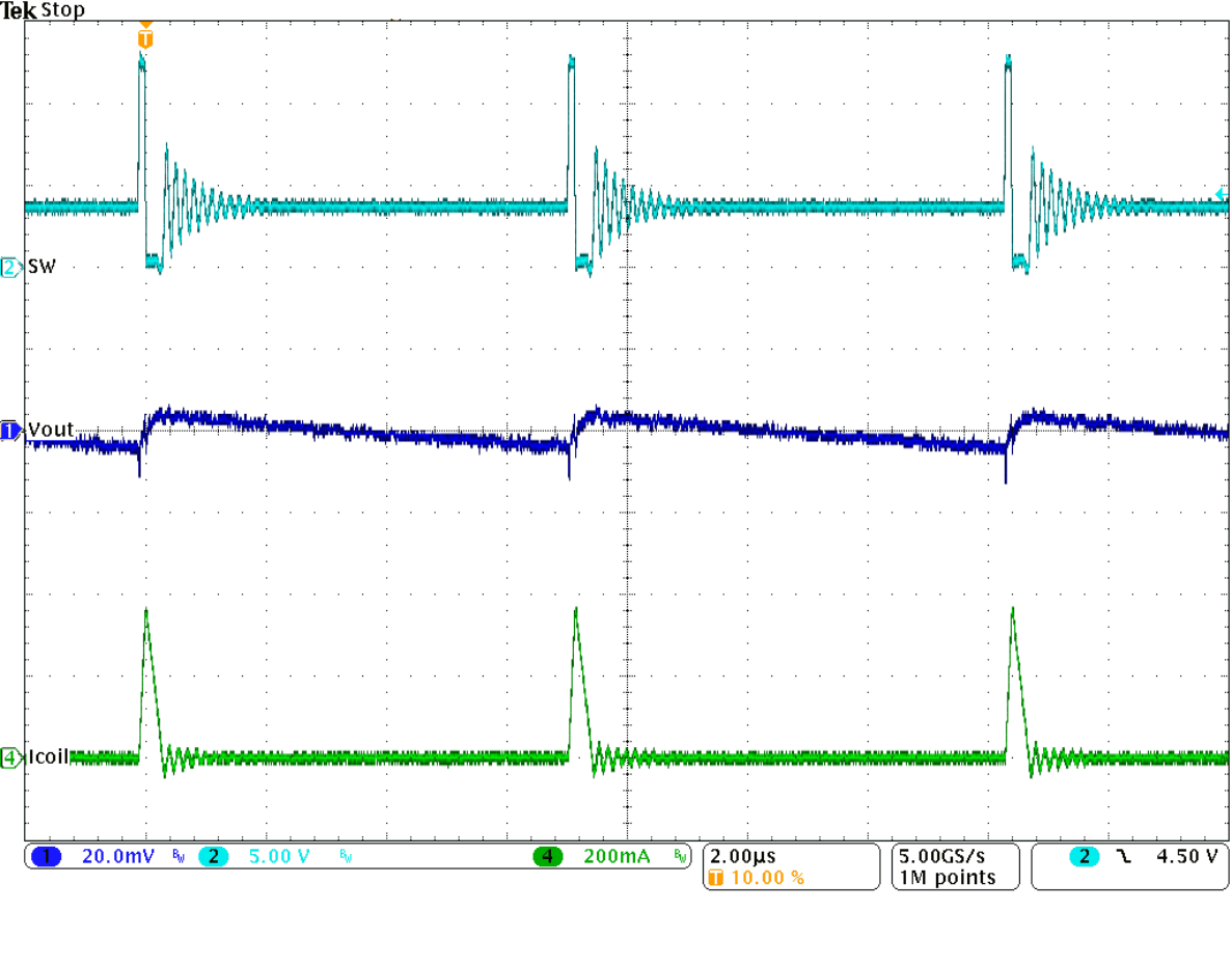
TPS62130A-Q1 TPS62133A-Q1 TPS6213013A-Q1 SLVSCC2_PSMtyp.gifFigure 36. Typical Operation in Power Save Mode (IOUT=10 mA)
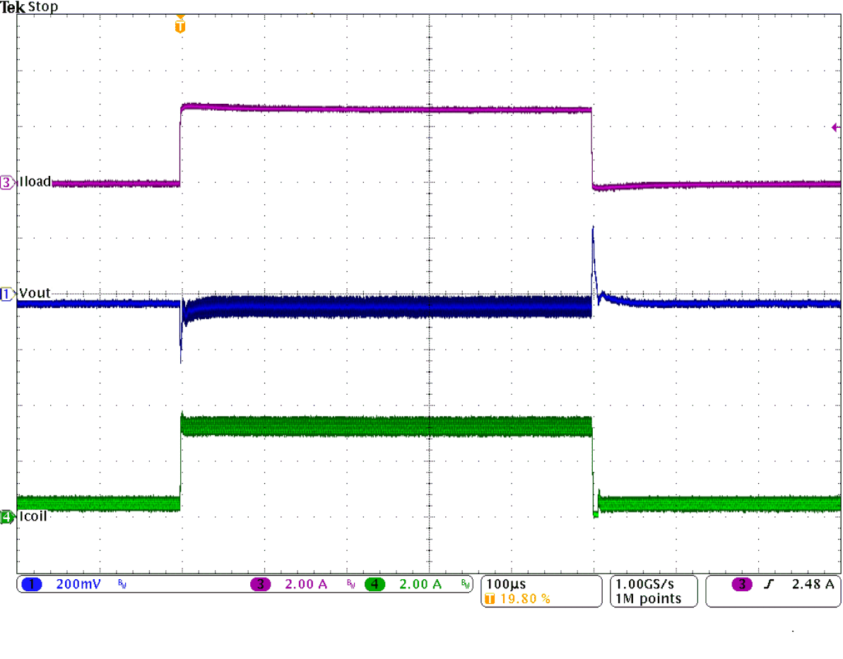
TPS62130A-Q1 TPS62133A-Q1 TPS6213013A-Q1 SLVSCC2_loadtranfull.gifFigure 38. Load Transient Response (0.5 to 3 to 0.5 A)
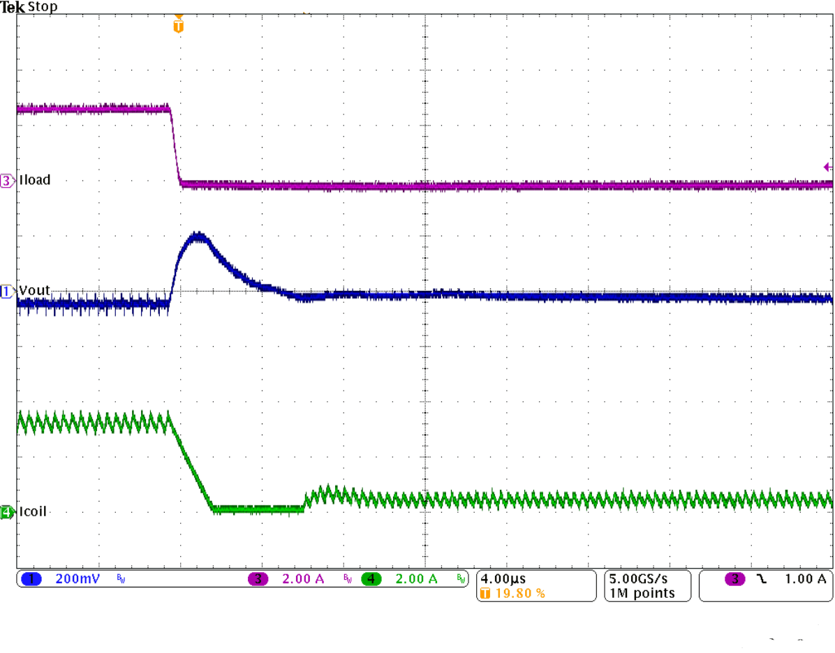
TPS62130A-Q1 TPS62133A-Q1 TPS6213013A-Q1 SLVSCC2_loadtranfall.gifFigure 40. Load Transient Response of Figure 38,
Falling Edge
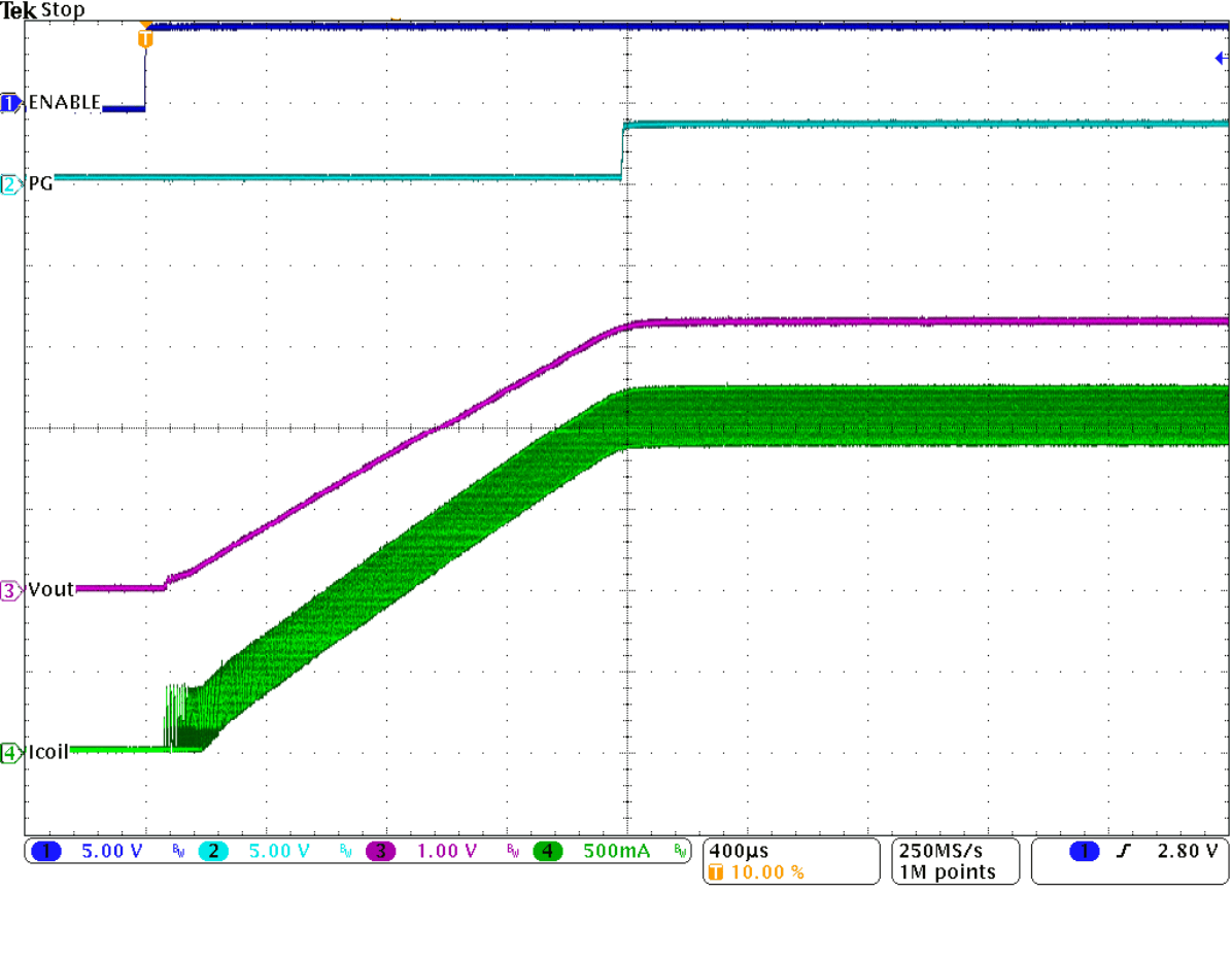
TPS62130A-Q1 TPS62133A-Q1 TPS6213013A-Q1 SLVSCC2_stuphigh.gifFigure 42. Start Up into 3 A