JAJS239G June 2007 – April 2018 TPS62290 , TPS62291 , TPS62293
PRODUCTION DATA.
- 1 特長
- 2 アプリケーション
- 3 概要
- 4 改訂履歴
- 5 Device Comparison Table
- 6 Pin Configuration and Functions
- 7 Specifications
- 8 Detailed Description
- 9 Application and Implementation
- 10Power Supply Recommendations
- 11Layout
- 12デバイスおよびドキュメントのサポート
- 13メカニカル、パッケージ、および注文情報
パッケージ・オプション
メカニカル・データ(パッケージ|ピン)
- DRV|6
サーマルパッド・メカニカル・データ
- DRV|6
発注情報
9.2.3 Application Curves
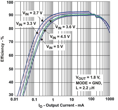 Figure 7. Efficiency (Power Save Mode) vs Output Current, VOUT = 1.8 V
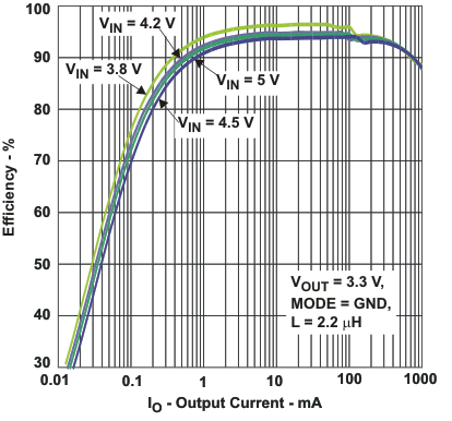 Figure 9. Efficiency (Power Save Mode) vs Output Current, VOUT = 3.3 V
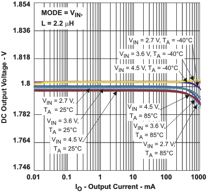 Figure 11. Output Voltage Accuracy (1.8-V Forced PWM Mode) vs Output Current
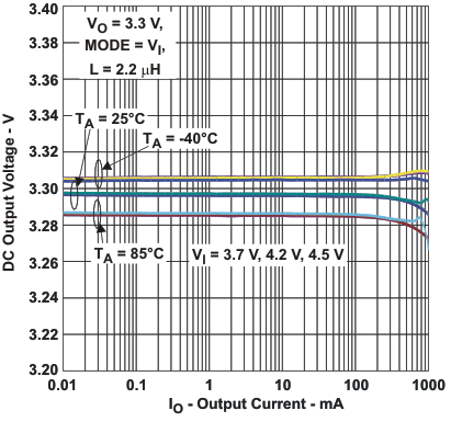 Figure 13. Output Voltage Accuracy 3.3-V Forced PWM Mode vs Output Current
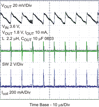 Figure 15. Typical Operation vs PFM Mode
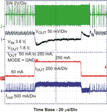 Figure 17. PFM Load Transient
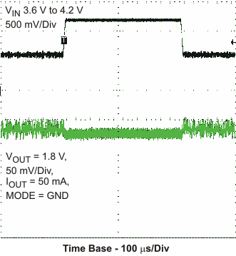 Figure 19. PWM Load Transient
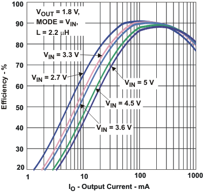 Figure 8. Efficiency (Forced PWM Mode) vs Output Current, VOUT = 1.8 V
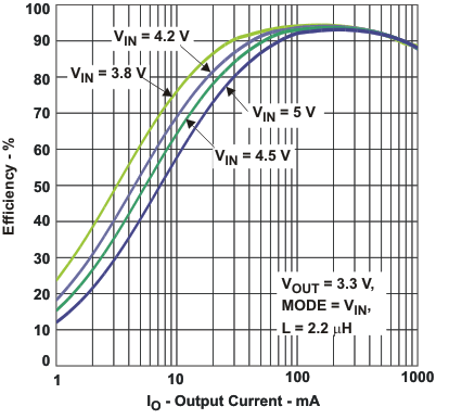 Figure 10. Efficiency (Forced PWM Mode) vs Output Current, VOUT = 3.3 V
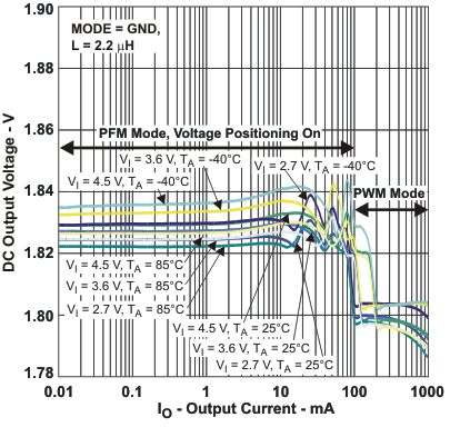 Figure 12. Output Voltage Accuracy (1.8-V Power Save Mode) vs Output Current
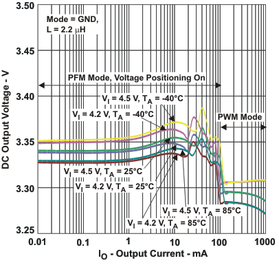 Figure 14. Output Voltage Accuracy 3.3-V Power Save Mode vs Output Current
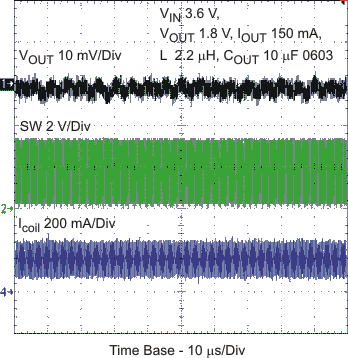 Figure 16. Typical Operation vs PWM Mode
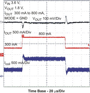 Figure 18. PFM Line Transient
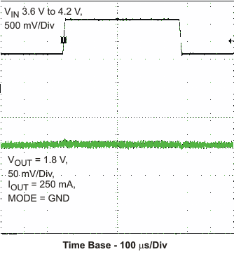 Figure 20. PWM Line Transient