JAJS360D January 2008 – October 2016 TPS62560 , TPS62561 , TPS62562
PRODUCTION DATA.
- 1 特長
- 2 アプリケーション
- 3 概要
- 4 改訂履歴
- 5 Device Comparison Table
- 6 Pin Configuration and Functions
- 7 Specifications
- 8 Detailed Description
- 9 Application and Implementation
- 10Power Supply Recommendations
- 11Layout
- 12デバイスおよびドキュメントのサポート
- 13メカニカル、パッケージ、および注文情報
パッケージ・オプション
メカニカル・データ(パッケージ|ピン)
- DRV|6
サーマルパッド・メカニカル・データ
- DRV|6
発注情報
6 Pin Configuration and Functions
DDC Package
5-Pin SOT
Top View

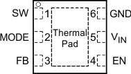
DRV Package
6-Pin SON
Top View

Pin Functions
| PIN | I/O | DESCRIPTION | ||
|---|---|---|---|---|
| NAME | No. QFN-6 |
No. TSOT23-5 |
||
| EN | 4 | 3 | I | This is the enable pin of the device. Pulling this pin to low forces the device into shutdown mode. Pulling this pin to high enables the device. This pin must be terminated. |
| FB | 3 | 4 | I | Feedback pin for the internal regulation loop. Connect the external resistor divider to this pin. In the fixed-output-voltage option, connect this terminal directly to the output capacitor. |
| GND | 6 | 2 | — | GND supply pin |
| MODE | 2 | N/A | I | This pin is only available as a QFN package option. MODE pin = high forces the device to operate in the fixed-frequency PWM mode. MODE pin = low enables the power-save mode with automatic transition from PFM mode to fixed-frequency PWM mode. |
| SW | 1 | 5 | O | This is the switch pin and is connected to the internal MOSFET switches. Connect the external inductor between this pin and the output capacitor. |
| VIN | 5 | 1 | — | VIN power-supply pin |
| Exposed Thermal Pad | — | N/A | — | Must be soldered to achieve appropriate power dissipation. Should be connected to GND. |