SLVS848D July   2009  – October 2015 TPS62620 , TPS62621 , TPS62622 , TPS62623 , TPS62624 , TPS62625

PRODUCTION DATA.  

  1. Features
  2. Applications
  3. Description
  4. Revision History
  5. Device Comparison Table
  6. Pin Configuration and Functions
  7. Specifications
    1. 7.1 Absolute Maximum Ratings
    2. 7.2 ESD Ratings
    3. 7.3 Recommended Operating Conditions
    4. 7.4 Thermal Information
    5. 7.5 Electrical Characteristics
    6. 7.6 Typical Characteristics
  8. Detailed Description
    1. 8.1 Overview
    2. 8.2 Functional Block Diagram
    3. 8.3 Feature Description
      1. 8.3.1 Mode Selection
      2. 8.3.2 Enable
      3. 8.3.3 Undervoltage Lockout
      4. 8.3.4 Thermal Shutdown
    4. 8.4 Device Functional Modes
      1. 8.4.1 Soft Start
      2. 8.4.2 Switching Frequency
      3. 8.4.3 Power-Save Mode
      4. 8.4.4 Output Capacitor Discharge (TPS62624 Only)
      5. 8.4.5 Short-Circuit Protection
  9. Application and Implementation
    1. 9.1 Application Information
    2. 9.2 Typical Application
      1. 9.2.1 Design Requirements
      2. 9.2.2 Detailed Design Procedure
        1. 9.2.2.1 Inductor Selection
        2. 9.2.2.2 Output Capacitor Selection
        3. 9.2.2.3 Input Capacitor Selection
        4. 9.2.2.4 Checking Loop Stability
      3. 9.2.3 Application Curves
  10. 10Power Supply Recommendations
  11. 11Layout
    1. 11.1 Layout Guidelines
    2. 11.2 Layout Example
    3. 11.3 Thermal Information
  12. 12Device and Documentation Support
    1. 12.1 Related Links
    2. 12.2 Community Resources
    3. 12.3 Trademarks
    4. 12.4 Electrostatic Discharge Caution
    5. 12.5 Glossary
  13. 13Mechanical, Packaging, and Orderable Information
    1. 13.1 Package Summary
    2. 13.2 Chip Scale Package Dimensions

パッケージ・オプション

メカニカル・データ(パッケージ|ピン)
サーマルパッド・メカニカル・データ
発注情報

13 Mechanical, Packaging, and Orderable Information

The following pages include mechanical, packaging, and orderable information. This information is the most current data available for the designated devices. This data is subject to change without notice and revision of this document. For browser-based versions of this data sheet, refer to the left-hand navigation.

13.1 Package Summary

CHIP SCALE PACKAGE
(BOTTOM VIEW)
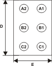
TPS62620 TPS62621 TPS62622 TPS62623 TPS62624 TPS62625 po_bott_lvs678.gif
CHIP SCALE PACKAGE
(TOP VIEW)
TPS62620 TPS62621 TPS62622 TPS62623 TPS62624 TPS62625 po_top_lvs848.gif
Code:
  • YM — Year Month date code
  • D — Day of Laser Mark
  • S — Assembly site code
  • CC — Chip code

13.2 Chip Scale Package Dimensions

The TPS6262x devices are available in an 6-bump chip scale package (YFF, NanoFree™). The package dimensions are given as:

  • D = 1.30 ±0.03 mm
  • E = 0.926 ±0.03 mm