SLVSAC3D May 2011 – December 2014 TPS62730 , TPS62732 , TPS62733
PRODUCTION DATA.
- 1 Features
- 2 Applications
- 3 Description
- 4 Revision History
- 5 Description (Continued)
- 6 Device Comparison Table
- 7 Pin Configuration and Functions
- 8 Specifications
- 9 Detailed Description
- 10Application and Implementation
- 11Power Supply Recommendations
- 12Layout
- 13Device and Documentation Support
- 14Mechanical, Packaging, and Orderable Information
パッケージ・オプション
メカニカル・データ(パッケージ|ピン)
- DRY|6
サーマルパッド・メカニカル・データ
- DRY|6
発注情報
9 Detailed Description
9.1 Overview
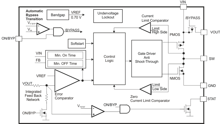
The TPS62730 combines a synchronous buck converter for high efficient voltage conversion and an integrated ultra low power bypass switch to support low power modes of modern micro controllers and RF ICs.
9.2 Functional Block Diagram

9.3 Feature Description
9.3.1 DCS-Control™
The TPS62730 includes TI's DCS-Control, an advanced regulation topology, that combines the advantages of hysteretic and voltage mode control architectures. While a comparator stage provides excellent load transient response, an additional voltage feedback loop ensures high DC accuracy as well. The DCS-Control enables switch frequencies up to 3 MHz, excellent transient and AC load regulation as well as operation with small and cost-competitive external components. The TPS6273x devices offer fixed output voltage options featuring smallest solution size by using only three external components. Furthermore this step-down converter provides excellent low output voltage ripple over the entire load range which makes this part ideal for RF applications. In the ultra low-power bypass mode, the output of the device VOUT is directly connected to the input VIN through the internal bypass switch. In this mode, the buck converter is shut down and consumes only 30 nA typical input current. Once the device is turned from ultra low-power bypass mode into buck converter operation for an RF transmission, all the internal circuits of the regulator are activated within a start up time tStart of typical 50 µs. During this time the bypass switch is still turned on and maintains the output VOUT connected to the input VIN. Once the DC-DC converter is settled and ready to operate, the internal bypass switch is turned off and the system is supplied by the output capacitor and the other decoupling capacitors. The buck converter kicks in once the capacitors connected to VOUT are discharged to the level of the nominal buck converter output voltage. Once the output voltage falls below the threshold of the internal error comparator, a switch pulse is initiated, and the high side switch of the DC-DC converter is turned on. The high-side switch remains turned on until a minimum on time of tONmin expires and the output voltage trips the threshold of the error comparator or the inductor current reaches the high side switch current limit. Once the high side switch turns off, the low side switch rectifier is turned on and the inductor current ramps down until the high side switch turns on again or the inductor current reaches zero. The converter operates in the PFM (pulse frequency modulation) mode during light loads, which maintains high efficiency over a wide load current range. In PFM mode, the device starts to skip switch pulses and generates only single pulses with the on time tONmin. The PFM mode of TPS62730 is optimized for low output ripple voltage if small external components are used.
The on time tONmin can be estimated to:

where
- tONmin: High side switch on time [ns]
- VIN: Input voltage [V]
- VOUT: Output voltage [V]
Therefore, the peak inductor current in PFM mode is approximately:

where
- VIN: Input voltage [V]
- VOUT: Output voltage [V]
- L : Inductance [μH]
- ILPFMpeak : PFM inductor peak current [mA]
9.3.2 ON/BYP Mode Selection
The DC-DC converter is activated when ON/BYP is set high. For proper operation, the ON/BYP pin must be terminated and may not be left floating. This pin is controlled by the RF transceiver or micro controller for proper mode selection. Pulling the ON/BYP pin low activates the ultra low-power bypass mode with typical 30-nA current consumption. In this mode, the internal bypass switch is turned on and the output of the DC-DC converter is connected to the battery VIN. All other circuits like the entire internal-control circuitry, the High Side and Low Side MOSFETs of the DC-DC output stage are turned off as well the internal resistor feedback divider is disconnected. The ON/BYP must be controlled by a microcontroller for proper mode selection. In case of CC2540, connect this to the power down signal which is output on one of the P1.x ports (see CC2540 user guide).
9.3.3 STAT Open-Drain Output
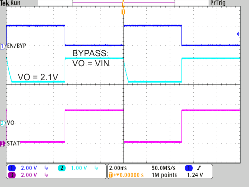
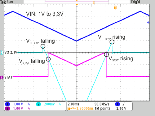
The STAT output is active when the device is enabled (EN/BYP = high) and indicates the status of the output voltage. The STAT output is a open-drain output with active low level and needs a external pullup resistor to indicate a high level. It is driven by an internal comparator which monitors the output voltage VOUT. The STAT pin is tied to low level, if the output voltage VOUT is considered as valid and exceeding the threshold VTSTAT (95% of VOUT for falling VIN and 98% of VOUT for rising VIN). The pin is high impedance with the ON/BYP pin set to low level or VOUT is below the VTSTAT threshold. If not used, the STAT pin can be left open. See Figure 6 and Figure 7.
 Figure 6. Operation Mode Transition ON/BYP = High/Low, RLoad = 1k
 Figure 7. STAT Pin / VOUT Behavior With EN/BYP = High, RLoad = 1k
9.4 Device Functional Modes
9.4.1 Start-Up
Once the device is supplied with a battery voltage, the bypass switch is activated. If the ON/BYP pin is set to high, the device operates in bypass mode until the DC-DC converter has settled and can kick in. During start-up, high peak currents can flow over the bypass switch to charge up the output capacitor and the additional decoupling capacitors in the system.
9.4.2 Automatic Transition from DC-DC to Bypass Operation
With the ON/BYP pin set to high, the TPS62730 is active and features an automatic transition between DC-DC and bypass mode to reduce the output ripple voltage to zero. Once the input voltage comes close to the output voltage of the DC-DC converter, the DC-DC converters operates close to 100% duty cycle operation. At this operating condition, the switch frequency would start to drop and would lead to increased output ripple voltage. The internal bypass switch is turned on once the battery voltage at VIN trips the Automatic Bypass Transition Threshold VIT BYP for falling VIN. The DC-DC regulator is turned off and therefore it generates no output ripple voltage. Due to the output is connected through the bypass switch to the input, the output voltage follows the input voltage minus the voltage drop across the internal bypass switch. In this mode the current consumption of the DC-DC converter is reduced to typically 23 µA. Once the input voltage increases and trips the bypass deactivation threshold VIT BYP for rising VIN, the DC-DC regulator turns on and the bypass switch is turned off. See Figure 7 and Figure 24.
9.4.3 Internal Current Limit
The TPS62730 integrates a High Side and Low Side MOSFET current limit to protect the device against heavy load or short circuit when the DC-DC converter is active. The current in the switches is monitored by current limit comparators. When the current in the High Side MOSFET reaches its current limit, the High Side MOSFET is turned off and the Low Side MOSFET is turned on to ramp down the current in the inductor. The High Side MOSFET switch can only turn on again, once the current in the Low Side MOSFET switch has fallen below the threshold of its current limit comparator. The bypass switch does not feature a current limit to support lowest current consumption.