JAJSCT0 December   2016 TPS63027

PRODUCTION DATA.  

  1. 特長
  2. アプリケーション
  3. 概要
  4. 標準アプリケーション
  5. 改訂履歴
  6. Device Comparison Table
  7. Pin Configuration and Functions
  8. Specifications
    1. 8.1 Absolute Maximum Ratings
    2. 8.2 ESD Ratings
    3. 8.3 Recommended Operating Conditions
    4. 8.4 Thermal Information
    5. 8.5 Electrical Characteristics
    6. 8.6 Timing Requirements
    7. 8.7 Typical Characteristics
  9. Detailed Description
    1. 9.1 Overview
    2. 9.2 Functional Block Diagram
    3. 9.3 Feature Description
      1. 9.3.1 Undervoltage Lockout (UVLO)
      2. 9.3.2 Output Discharge Function
      3. 9.3.3 Thermal Shutdown
      4. 9.3.4 Softstart
      5. 9.3.5 Short Circuit Protection
    4. 9.4 Device Functional Modes
      1. 9.4.1 Control Loop Description
      2. 9.4.2 Power Save Mode Operation
      3. 9.4.3 Current Limit
      4. 9.4.4 Supply and Ground
      5. 9.4.5 Device Enable
  10. 10Application and Implementation
    1. 10.1 Application Information
    2. 10.2 Typical Applications
      1. 10.2.1 Design Requirements
      2. 10.2.2 Detailed Design Procedure
        1. 10.2.2.1 Output Filter Design
        2. 10.2.2.2 Inductor Selection
        3. 10.2.2.3 Capacitor Selection
          1. 10.2.2.3.1 Input Capacitor
          2. 10.2.2.3.2 Output Capacitor
        4. 10.2.2.4 Setting The Output Voltage
      3. 10.2.3 Application Curves
  11. 11Power Supply Recommendations
  12. 12Layout
    1. 12.1 Layout Guidelines
    2. 12.2 Layout Example
  13. 13デバイスおよびドキュメントのサポート
    1. 13.1 デバイス・サポート
      1. 13.1.1 デベロッパー・ネットワークの製品に関する免責事項
    2. 13.2 ドキュメントのサポート
      1. 13.2.1 関連資料
    3. 13.3 ドキュメントの更新通知を受け取る方法
    4. 13.4 コミュニティ・リソース
    5. 13.5 商標
    6. 13.6 静電気放電に関する注意事項
    7. 13.7 用語集
  14. 14メカニカル、パッケージ、および注文情報

パッケージ・オプション

メカニカル・データ(パッケージ|ピン)
サーマルパッド・メカニカル・データ
発注情報

Layout

Layout Guidelines

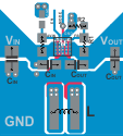
The PCB layout is an important step to maintain the high performance of the TPS63027 devices.

  • Place input and output capacitors as close as possible to the IC. Traces need to be kept short. Routing wide and direct traces to the input and output capacitor results in low trace resistance and low parasitic inductance.
  • Use a common-power GND
  • Use separate traces for the supply voltage of the power stage; and, the supply voltage of the analog stage.
  • The sense trace connected to FB is signal trace. Keep these traces away from L1 and L2 nodes.

Layout Example

TPS63027 TPS63027_ds_layout2.gif Figure 21. TPS63027 Layout