JAJSNI5A december 2022 – august 2023 TPS631010 , TPS631011
PRODUCTION DATA
- 1
- 1 特長
- 2 アプリケーション
- 3 概要
- 4 Revision History
- 5 Device Comparison Table
- 6 Pin Configuration and Functions
- 7 Specifications
-
8 Detailed Description
- 8.1 Overview
- 8.2 Functional Block Diagram
- 8.3 Feature Description
- 8.4 Device Functional Modes
- 9 Application and Implementation
- 10Device and Documentation Support
- 11Mechanical, Packaging, and Orderable Information
8.3.2 Enable and Soft Start
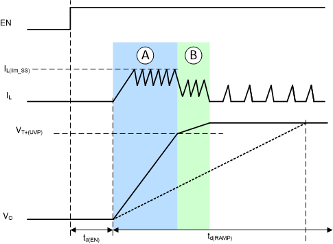
 Figure 8-1 Typical Soft-Start Behavior
When the input voltage is above the UVLO rising threshold and the EN pin is pulled to a voltage above 1.2 V, the TPS631010 and TPS631011 are enabled and start up after a short delay time, td(EN).
The devices have an inductor peak current clamp to limit the inrush current during start-up. When the minimum current clamp (IL(lim_SS)) is lower than the current that is necessary to follow the voltage ramp, the current automatically increases to follow the voltage ramp. The minimum current limit ensures as fast as possible soft start if the capacitance is chosen lower than what the ramp time td(RAMP) was selected for.
In a typical start-up case as shown in Figure 8-1 (low output load, typical output capacitance), the minimum current clamp limits the inrush current and charges the output capacitor. The output voltage then rises faster than the reference voltage ramp (see phase A in Figure 8-1). To avoid an output overshoot, the current clamp is deactivated when the output is close to the target voltage and follows the reference voltage ramp slew value given by the voltage ramp, which is finishing the start up (see phase B in Figure 8-1). The transition from the minimum current clamp operation is sensed by using the threshold VT+(UVP), which is typically 90% of the target output voltage. After phase B, the output voltage is well regulated to the nominal target voltage. The current waveform depends on the output load and operation mode.