JAJSGI0D November   2018  – January 2021 TPS63802

PRODUCTION DATA  

  1. 特長
  2. アプリケーション
  3. 概要
  4. Revision History
  5. 概要 (続き)
  6. Device Comparison Table
  7. Pin Configuration and Functions
  8. Specifications
    1. 8.1 Absolute Maximum Ratings
    2. 8.2 ESD Ratings
    3. 8.3 Recommended Operating Conditions
    4. 8.4 Thermal Information
    5. 8.5 Electrical Characteristics
    6. 8.6 Typical Characteristics
  9. Detailed Description
    1. 9.1 Overview
    2. 9.2 Functional Block Diagram
    3. 9.3 Feature Description
      1. 9.3.1  Control Loop Description
      2. 9.3.2  Precise Device Enable: Threshold- or Delayed Enable
      3. 9.3.3  Mode Selection (PFM/PWM)
      4. 9.3.4  Undervoltage Lockout (UVLO)
      5. 9.3.5  Soft Start
      6. 9.3.6  Adjustable Output Voltage
      7. 9.3.7  Overtemperature Protection - Thermal Shutdown
      8. 9.3.8  Input Overvoltage - Reverse-Boost Protection (IVP)
      9. 9.3.9  Output Overvoltage Protection (OVP)
      10. 9.3.10 Power-Good Indicator
    4. 9.4 Device Functional Modes
      1. 9.4.1 Peak-Current Mode Architecture
        1. 9.4.1.1 Reverse Current Operation, Negative Current
        2. 9.4.1.2 Boost Operation
        3. 9.4.1.3 Buck-Boost Operation
        4. 9.4.1.4 Buck Operation
      2. 9.4.2 Power Save Mode Operation
        1. 9.4.2.1 Current Limit Operation
  10. 10Application and Implementation
    1. 10.1 Application Information
    2. 10.2 Typical Application
      1. 10.2.1 Design Requirements
      2. 10.2.2 Detailed Design Procedure
        1. 10.2.2.1 Custom Design With WEBENCH® Tools
        2. 10.2.2.2 Inductor Selection
        3. 10.2.2.3 Output Capacitor Selection
        4. 10.2.2.4 Input Capacitor Selection
        5. 10.2.2.5 Setting The Output Voltage
      3. 10.2.3 Application Curves
  11. 11Power Supply Recommendations
  12. 12Layout
    1. 12.1 Layout Guidelines
    2. 12.2 Layout Example
  13. 13Device and Documentation Support
    1. 13.1 Device Support
      1. 13.1.1 Third-Party Products Disclaimer
      2. 13.1.2 Development Support
        1. 13.1.2.1 Custom Design With WEBENCH® Tools
    2. 13.2 Documentation Support
      1. 13.2.1 Related Documentation
    3. 13.3 ドキュメントの更新通知を受け取る方法
    4. 13.4 サポート・リソース
    5. 13.5 Trademarks
    6. 13.6 静電気放電に関する注意事項
    7. 13.7 用語集
  14. 14Mechanical, Packaging, and Orderable Information

パッケージ・オプション

メカニカル・データ(パッケージ|ピン)
サーマルパッド・メカニカル・データ
発注情報

Undervoltage Lockout (UVLO)

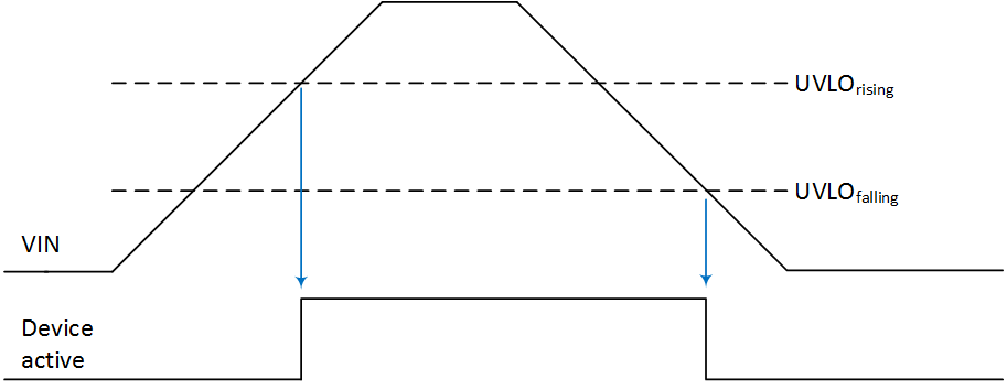
To avoid mis-operation of the device at low input voltages, an undervoltage lockout is included. It activates the device once the input voltage (VI) has increased the UVLOrising value. Once active, the device allows operation down to even smaller input voltages, which is determined by the UVLOfalling. This behavior requires VO to be higher than the minimum value of 1.8 V.
GUID-B0667F47-77C5-458E-A598-B5E6B5004A99-low.gifFigure 9-3 Rising and Falling Undervoltage Lockout Behavior